Flash Lamp Annealing (eBook)
XVIII, 288 Seiten
Springer International Publishing (Verlag)
978-3-030-23299-3 (ISBN)
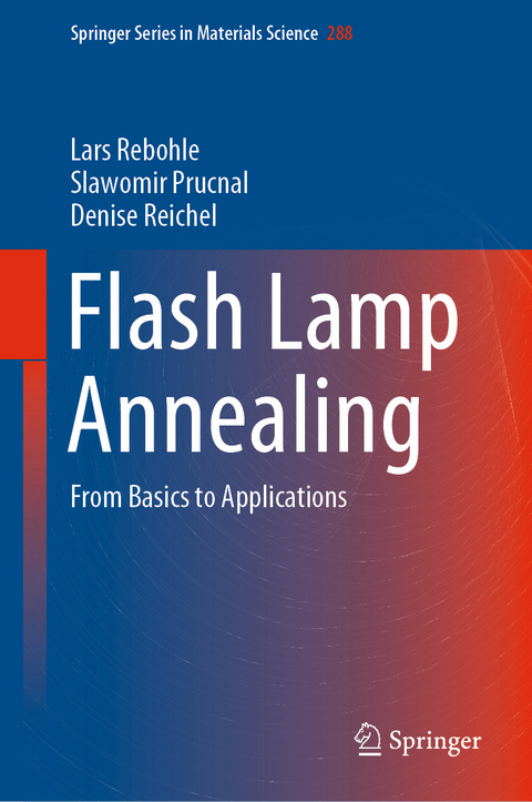
This book provides a comprehensive survey of the technology of flash lamp annealing (FLA) for thermal processing of semiconductors. It gives a detailed introduction to the FLA technology and its physical background. Advantages, drawbacks and process issues are addressed in detail and allow the reader to properly plan and perform their own thermal processing. Moreover, this books gives a broad overview of the applications of flash lamp annealing, including a comprehensive literature survey. Several case studies of simulated temperature profiles in real material systems give the reader the necessary insight into the underlying physics and simulations. This book is a valuable reference work for both novice and advanced users.
Lars Rebohle received a Diplom in physics from the Technical University of Dresden in 1995. From 1996 to 2001 he was employed at the Dresden-Rossendorf Research Centre, now Helmholtz-Zentrum Dresden-Rossendorf (HZDR), working on the luminescence properties of ion-implanted, nanocrystalline SiO2 layers. He received his Ph.D. in 1999. After a post-doctoral stay at the Technical University in Vienna in 2002, he worked from 2003 to 2006 in industry dealing with ion implantation, flash lamp annealing and thin film deposition. Since 2007, he has been working as a scientist at the HZDR and engaged in research on Si-based light emitters with rare earth elements. His current research topics include the doping, crystallization and annealing of semiconductor materials and nanostructures in non-thermal equilibrium. From 2010 to 2015 he was guest lecturer at the Technical University Bergakademie Freiberg, where he got his habilitation in 2013.
Slawomir Prucnal received a Diplom in physics from the University of Maria Curie-Sklodowska in Lublin, Poland in 2008. From 2008 he as been employed at the HZDR, working on the optoelectronic properties of ion-implanted semiconductors (group IV and III-V), both on bulk and nanostructures. From 2009 to 2011 he carried out postdoctoral work at the TU Bergakademie Freiberg, Institute for Experimental Physics as part of a Cluster of Excellence project, focused on the development of solar cells. His current research topics include hyperdoped semiconductors (e.g. SiSe), ultra-doped Ge for superconductivity and MID plasmonics, defects and doping engineering in Transparent Conductive Oxides (TCOs).
Denise Reichel received an interdisciplinary Bachelor of Science in 2005 from the University of Newcastle-upon Tyne, United Kingdom. Thereafter, she continued her studies in applied natural science at the Technical University Bergakademie Freiberg to receive her Diplom in 2008. From 2009 to 2013 she worked at the HZDR in the field of temperature measurement during flash lamp annealing. After a short detour to science communication she has been continuing her scientific career at the AKAD University of Applied Sciences in Stuttgart as a lecturer and tutor in the field of thermodynamics from 2014 until today. In addition she is working as a consultant in technical sales for the pyrometer manufacturer Sensortherm since 2015. She received her Ph.D. in February 2015 and continues studying temperature measurement during lamp-based processing.Preface 6
Acknowledgements 7
References 8
Contents 9
Acronyms 12
Symbols 14
1 Introduction 18
1.1 Historical Remarks 19
1.2 The Thermal Cycle 24
1.3 Short Time Annealing 26
References 28
2 The Technology of Flash Lamp Annealing 32
2.1 Basic Structure of an FLA Tool 32
2.2 Components of a Flash Lamp 36
2.2.1 Dimensions and Gas Filling 37
2.2.2 Electrodes 38
2.2.3 The Envelope 40
2.2.4 Cooling 42
2.3 Plasma Discharge 43
2.3.1 Trigger Pulse and Initial Streamer Formation 43
2.3.2 Arc Expansion 46
2.3.3 Plasma Properties in the Wall-Stabilized Regime 48
2.3.4 The Post-discharge Period 54
2.4 Electric Operation 55
2.4.1 Electric Characteristics of a Flash Lamp 55
2.4.2 Circuitries 56
2.4.3 Modelling of a Single RLC Section Circuit 59
2.4.4 Active Pulse Shaping 62
2.5 Optical Output 64
2.5.1 The Plasma Spectrum 64
2.5.2 Transparency and Radiation Pattern 66
2.5.3 Time-Resolved Optical Properties 68
2.5.4 Shaping the Spectral Output 68
2.6 Flash Lamp Lifetime 72
2.6.1 Single and Multiple Flash Operation 72
2.6.2 Lamp Failure 73
2.6.3 Lamp Degradation 77
2.7 Layout of FLA Tools 79
2.7.1 From Sheet-to-Sheet to Roll-to-Roll Processes 79
2.7.2 Flash-Assisted Deposition 81
References 84
3 Process Management 88
3.1 Temperature Measurement 88
3.1.1 Pyrometry 89
3.1.2 Temperature Measurement of Semiconductors 91
3.1.3 Temperature Measurement During Annealing of Non-semiconductors 101
3.1.4 True Temperature Measurement 103
3.2 Temperature Simulations 106
3.2.1 Mathematical Background 106
3.2.2 Chamber Wall Reflection 111
3.2.3 Temperature Profiles 115
3.2.4 Heat Dissipation 121
3.3 Homogeneity 123
3.3.1 The Homogeneity of Irradiation 123
3.3.2 Pattern Effects 128
3.4 Thermal Stress 131
3.4.1 Silicon 131
3.4.2 Glassy Substrates and Thin Films 136
3.5 Further Effects 138
References 142
4 Semiconductor Applications 147
4.1 Defect Engineering 147
4.1.1 Defect Evolution During Annealing 147
4.1.2 Boron Diffusion in Si 149
4.1.3 Studies Related to Flash Lamp Annealing 151
4.2 Doping 152
4.2.1 Ultra-Shallow Junctions in Silicon 152
4.2.2 Hyperdoping in Silicon 160
4.2.3 Doping and Superconductivity in Germanium 167
4.2.4 Doping of Silicon Carbide 179
4.2.5 Doping of III–V Compound Semiconductors 184
4.2.6 Diluted Magnetic Semiconductors 190
4.3 Crystallization 194
4.3.1 Non-equilibrium Crystallization Modes 194
4.3.2 Thin Films of Amorphous Silicon 202
4.3.3 Silicon Compound Semiconductors 206
4.4 Semiconductor Nanostructures 210
4.4.1 Group IV Nanocluster 210
4.4.2 Integration of III–V Nanocrystals into Silicon 212
4.4.3 Nanowires 224
References 234
5 Beyond Semiconductors 249
5.1 Dielectric Thin Films 249
5.1.1 High-k Materials 249
5.1.2 Rare Earth Doping of SiO2 251
5.2 Photovoltaic Applications 253
5.2.1 Mono- and Polycrystalline Solar Cells 254
5.2.2 Thin Film Solar Cells 258
5.3 Transparent Conducting Oxides 260
5.3.1 Zinc Oxide 260
5.3.2 Titanium Oxide 263
5.3.3 Indium Tin Oxide 264
5.3.4 Other TCOs and Beyond 266
5.4 Metallic Films 267
5.4.1 Annealing of Thin Metal Films 268
5.4.2 Material Property Engineering 269
5.4.3 Silicides 269
5.4.4 Printed Electronics 271
5.4.5 Further Applications 272
5.5 Flexible Substrates 273
5.5.1 State of the Art 274
5.5.2 Ink-Environment Interaction 285
5.5.3 Ink-Substrate Interaction 287
References 289
Index 299
| Erscheint lt. Verlag | 27.7.2019 |
|---|---|
| Reihe/Serie | Springer Series in Materials Science |
| Zusatzinfo | XVIII, 288 p. |
| Sprache | englisch |
| Themenwelt | Technik ► Elektrotechnik / Energietechnik |
| Technik ► Maschinenbau | |
| Wirtschaft ► Betriebswirtschaft / Management ► Logistik / Produktion | |
| Schlagworte | FLA assisted deposition • High-K dielectrics • High-k Materials • Millisecond annealing • Semiconductor Nanostructures • Transparent conducting oxides |
| ISBN-10 | 3-030-23299-9 / 3030232999 |
| ISBN-13 | 978-3-030-23299-3 / 9783030232993 |
| Haben Sie eine Frage zum Produkt? |
Größe: 13,4 MB
DRM: Digitales Wasserzeichen
Dieses eBook enthält ein digitales Wasserzeichen und ist damit für Sie personalisiert. Bei einer missbräuchlichen Weitergabe des eBooks an Dritte ist eine Rückverfolgung an die Quelle möglich.
Dateiformat: PDF (Portable Document Format)
Mit einem festen Seitenlayout eignet sich die PDF besonders für Fachbücher mit Spalten, Tabellen und Abbildungen. Eine PDF kann auf fast allen Geräten angezeigt werden, ist aber für kleine Displays (Smartphone, eReader) nur eingeschränkt geeignet.
Systemvoraussetzungen:
PC/Mac: Mit einem PC oder Mac können Sie dieses eBook lesen. Sie benötigen dafür einen PDF-Viewer - z.B. den Adobe Reader oder Adobe Digital Editions.
eReader: Dieses eBook kann mit (fast) allen eBook-Readern gelesen werden. Mit dem amazon-Kindle ist es aber nicht kompatibel.
Smartphone/Tablet: Egal ob Apple oder Android, dieses eBook können Sie lesen. Sie benötigen dafür einen PDF-Viewer - z.B. die kostenlose Adobe Digital Editions-App.
Zusätzliches Feature: Online Lesen
Dieses eBook können Sie zusätzlich zum Download auch online im Webbrowser lesen.
Buying eBooks from abroad
For tax law reasons we can sell eBooks just within Germany and Switzerland. Regrettably we cannot fulfill eBook-orders from other countries.
aus dem Bereich
