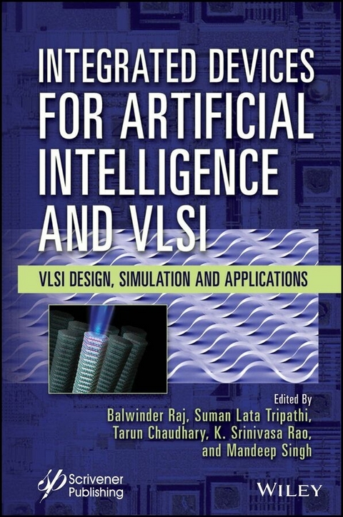
Integrated Devices for Artificial Intelligence and VLSI (eBook)
592 Seiten
Wiley-Scrivener (Verlag)
978-1-394-20513-4 (ISBN)
With its in-depth exploration of the close connection between microelectronics, AI, and VLSI technology, this book offers valuable insights into the cutting-edge techniques and tools used in VLSI design automation, making it an essential resource for anyone seeking to stay ahead in the rapidly evolving field of VLSI design.
Very large-scale integration (VLSI) is the inter-disciplinary science of utilizing advanced semiconductor technology to create various functions of computer system. This book addresses the close link of microelectronics and artificial intelligence (AI). By combining VLSI technology, a very powerful computer architecture confinement is possible. To overcome problems at different design stages, researchers introduced artificial intelligent (AI) techniques in VLSI design automation. AI techniques, such as knowledge-based and expert systems, first try to define the problem and then choose the best solution from the domain of possible solutions.
These days, several CAD technologies, such as Synopsys and Mentor Graphics, are specifically created to increase the automation of VLSI design. When a task is completed using the appropriate tool, each stage of the task design produces outcomes that are more productive than typical. However, combining all of these tools into a single package offer has drawbacks. We can't really use every outlook without sacrificing the efficiency and usefulness of our output. The researchers decided to include AI approaches into VLSI design automation in order to get around these obstacles. AI is one of the fastest growing tools in the world of technology and innovation that helps to make computers more reliable and easy to use. Artificial Intelligence in VLSI design has provided high-end and more feasible solutions to the difficulties faced by the VLSI industry. Physical design, RTL design, STA, etc. are some of the most in-demand courses to enter the VLSI industry. These courses help develop a better understanding of the many tools like Synopsis. With each new dawn, artificial intelligence in VLSI design is continually evolving, and new opportunities are being investigated.
Balwinder Raj, PhD, is an associate professor in the Electronics and Communication Engineering Department, at the National Institute of Technical Teachers Training and Research, Chandigarh. He has published more than 100 research papers in national and international journals and conferences. Additionally, the European Commission awarded him a Mobility of Life research fellowship for postdoc research work at the University of Rome, Tor Vergata, Italy in 2010-2011. His areas of interest include nanoscale semiconductor device modeling, sensors design, FinFET-based memory design, and low-power VLSI design.
Suman Lata Tripathi, PhD, is a professor at the Lovely Professional University with more than 20 years of experience in academics. She is also a remote post-doctoral researcher at Nottingham Trent University, London, UK. She has published more than 74 research papers in refereed science journals and conferences, as well as 13 Indian patents and two copyrights. Additionally, she has edited and authored more than 17 books in different areas of electronics and electrical engineering.
Tarun Chaudhary, PhD, is an assistant professor in the Electronics and Communication Engineering Department at the Dr. B.R. Ambedkar National Institute of Technology, Jalandhar, India. During her PhD, she worked on the design and mathematical modeling of the vertical field effect transistor. She has five book chapters and more than 25 research papers in peer-reviewed national and international journals and conferences.
K. Srinivasa Rao, PhD, is a professor and the head of the Microelectronics Research Group in the Department of Electronics and Communication Engineering at the Koneru Lakshmaiah Education Foundation, Andhra Pradesh, India. His areas of research include MEMS-based reconfigurable antennas, MEMS actuators, piezoresistive, and VLSI circuts. He is a reviewer for many SCI-indexed journals and an external reviewer for many universities.
Mandeep Singh is a professor at the Indian Institute of Information Technology, Surat Gujarat. He has five years of teaching experience with undergraduate and master students. He has published various research papers in the domain of VLSI design and circuits.
Preface
The current research trend in Integrated Semiconductor Devices for Artificial Intelligence and Very Large Scale Integration (VLSI) is exploring the potential of device and artificial intelligence for emerging engineering applications. In the current Integrated Circuits, switching time is on the order of nanoseconds, minimum feature size is on the order of nanometers, transistor count is on the order of billions and cost is on the order of a few dollars. Scaling of conventional MOSFETs towards smaller sizes is near to end because of limited mobility, large Short Channel Effects (SCEs), high leakage currents and power dissipation. To mitigate these challenges of conventional MOSFET devices and to scale the semiconductor device further into nanoscale domain, alternative materials and device structures are required. There are numerous challenges in the development of models for distributed intelligence systems for environmental monitoring, but these can be mitigated with artificial intelligence, machine learning, and deep learning. This book will help identify the areas where we encounter numerous challenges and apply diverse solutions for the development of advanced Integrated Devices for Artificial Intelligence and VLSI.
Chapter 1: The chapter 1 offers a thorough comparison of the two well-known transistor designs, MOSFET and FinFET, which have revolutionized integrated circuit architecture. The chapter offers a thorough investigation of the core ideas, design factors, and operational traits between the two transistor techniques. It describes the development of MOSFET technologies and how it has significantly advanced current electronics. The drawbacks of conventional MOSFET scaling are brought to light, necessitating the use of FinFET and other innovative transistor architectures. FinFET, revealing its ground-breaking design with a channel shaped like a fin and many gates. It examines the special operational benefits of FinFET, such as greater device scalability, improved electrostatic control, and lower leakage current. The article also looks at difficulties in designing and producing FinFETs, such as increasing process complexity and unpredictability. The outcomes of MOSFET and FinFET are compared and contrasted over a number of important factors. These factors involve switching speed, noise immunity, power efficiency, power dissipation, leakage current, on-state current, subthreshold slope, threshold voltage control, and device scaling.
Chapter 2: Improvements in the VLSI industry have always been striving to justify the Moore’s law by implanting, twice count transistors from the existing one. This law has made a significant improvement in the trends of FET family starting with the straightforward MOSFET with one gate controlling the channel, then next followed by FET with Dual gates, later Tri-gate/Fin FET and now persisting Gate-All-Around Field Effect Transistor. Each era of technology contributed its own advantages and disadvantages. Presently the Gate-All-Around FETs are ruling the FET industry because of its major advantage of improved gate electrostatic integrity over the channel from all the directions, with reduced overall size of the FET. In this research work, the vertically stacked GAA Nanosheet FET is simulated at the device-level using Visual TCAD – 3D Cogenda tool. Research is conducted to substantiate the influence of geometrical variations with respect to thickness and width on the performance of the FET. Parameters analyzed to in the research are ION, IOFF, Switching ratio (ION/IOFF), Subthreshold swing (SS), DIBL, and Threshold voltage (Vth). Device is optimal if it offers better ON current, minimum OFF current. To evaluate this optimal performance the thickness of the nanosheet (NT) is varied from 5nm to 9nm, and the width is varied from 10nm to 50nm. Visual TCAD - 3D Cogenda tool is used in analyzing the outputs generated and conclude the best geometric dimension for optimum characteristics.
Chapter 3: The standard MOSFET used in modern IC technology is expected to be replaced by new tunnel fieldeffect transistor (TFET), which is seen to be the utmost viable contender. Researchers have been very interested in it as a result of it’s capacity to attain a steep sub-threshold slope, a stronger resilience to shortchannel effect’s, and a reduced standby power dissipation. The current transport technique, band to band tunnelling (BTBT), causes TFET’s two main bottlenecks, lower Ion current and ambipolar conductivity, despite the fact that it promises several benefits over other MOSFET competitors. This article provides a thorough overview of the many methods researchers have proposed to increase the ON-State current and subthreshold swing in Tunnel FETs.
Chapter 4: The unique characteristics of nanowire field effect transistors (NW FETs), such as high electron mobility, low power consumption, and scalability, have made them a promising technology for upcoming electronic devices. An overview of the underlying concepts, methods of fabrication, and performance traits of NW FETs are given in this chapter. The chapter discusses the benefits and drawbacks of NW FETs, including how contact resistance, defect density, and surface effects affect device performance. The chapter also highlights the potential uses of NW FETs in several industries, including sensing, computing, and energy harvesting. Overall, this chapter offers a thorough reference for researchers and engineers interested in this innovative technology since NW FETs are anticipated to play a significant role in the creation of next-generation electronic devices.
Chapter 5: The Moore law for scaling of technological nodes has led to the major advancement in chip design and functionality. With the downscaling of technological nodes, the efficiency of gate becomes insignificant compared to the interconnect performance. The reliability issue play a major role at nano-scaled technological nodes since future interconnects requires higher current density with compact cross-sectional dimensions. Formerly, copper was employed as interconnect due to high current density and less resistivity but as technology downscales below 45nm its resistance increases due to the reduction of MFP. The scaling of interconnect dimensions effects the delay time as well as power dissipation. The electronics circuit operational speed is affected by the signal delay at the output of wire. The power dissipation is also a key factor in VLSI ICs. In today’s world, everyone demands higher power standby and speed in electronic circuits. The motivation for minimizing delay in signal and power dissipation at global lengths for various technological nodes varies according to applications. The overall performance of electronic circuit depends on the product of power dissipation and delay. Both are independent parameters but to estimate actual performance of an interconnect their product must be taken into account for elite integrated circuits. This chapter has proposed MLGNR as suitable and alternative material in on-chip interconnects for future technological nodes compared to copper interconnects.
Chapter 6: We examine the recent development of ferroelectric memory, along with ferroelectric random access memory (FRAM). Sophisticated non-volatile memories including resistive random access memory (ReRAM), phase-change random access memory (PRAM), and magnetoresistive random access memory (MRAM) have all been expanded, but FRAM is the first of these to be commercially available. Currently, a few Mb of extremely dependable FRAM is accessible. FRAM has been used in sophisticated smartcards, RFID tags, and other electronic devices because of its superior electric features, which include fast read/write speeds around 50 ns, low power consumption, and high switching durability around 1013. We also discuss recently created materials, manufacturing techniques, and circuit technologies that are anticipated to solve the scalability issue with FRAM.
Chapter 7: Very large-scale integration (VLSI) is the process of combining a large number of transistors on a single chip to form an integrated circuit. VLSI development is rapidly moving toward the efficient design of a single chip. However, VLSI design faces numerous challenges, including power optimization, design productivity, manufacturing variability and testability. Conventional methodologies are primarily manual, timeconsuming and resource-intensive. Artificial Intelligence (AI) and Machine Learning (ML) techniques, on the other hand, provide automated learning approaches for dealing with large amounts of data in complex chip design. Furthermore, incorporating machine learning algorithms can improve system-on-chip performance. AI/ML is becoming more important in VLSI design due to its numerous applications in both logical and physical design. As a result, AI/ML has become an essential component in the VLSI industry. This chapter discusses popular ML algorithms, their mathematical foundations, performance metrics, and how AI and ML applications can transform VLSI design by allowing for high-speed, intelligent and efficient implementations.
Chapter 8: A computing device is deemed rudimentary if its operational scope is confined to elementary high-school-level mathematical tasks. Conversely, a mechanism that incorporates components of biotic origin, like as DNA units, as opposed to conventional electrical elements, closely mirrors the intricacies of the human brain. The instantiation of a computation system that operates neurons and synapses in parallel, exhibiting high capacity and low power consumption, constitutes a neuromorphic computing system (NCS). Neurons communicate through the transmission of...
| Erscheint lt. Verlag | 1.8.2024 |
|---|---|
| Sprache | englisch |
| Themenwelt | Technik ► Elektrotechnik / Energietechnik |
| Schlagworte | CNTFET • Double Gate MOSFET • FinFET • FPGA Design • Gate All Around Devices • III-V Compound Devices • nano MOSFET • NanoTube FET • nanowire • Semiconductor Devices • Short channel effects • TFET • VLSI Architecture • VLSI Design Methodologies • VLSI Hardware Implementation |
| ISBN-10 | 1-394-20513-9 / 1394205139 |
| ISBN-13 | 978-1-394-20513-4 / 9781394205134 |
| Haben Sie eine Frage zum Produkt? |
Größe: 32,1 MB
Kopierschutz: Adobe-DRM
Adobe-DRM ist ein Kopierschutz, der das eBook vor Mißbrauch schützen soll. Dabei wird das eBook bereits beim Download auf Ihre persönliche Adobe-ID autorisiert. Lesen können Sie das eBook dann nur auf den Geräten, welche ebenfalls auf Ihre Adobe-ID registriert sind.
Details zum Adobe-DRM
Dateiformat: EPUB (Electronic Publication)
EPUB ist ein offener Standard für eBooks und eignet sich besonders zur Darstellung von Belletristik und Sachbüchern. Der Fließtext wird dynamisch an die Display- und Schriftgröße angepasst. Auch für mobile Lesegeräte ist EPUB daher gut geeignet.
Systemvoraussetzungen:
PC/Mac: Mit einem PC oder Mac können Sie dieses eBook lesen. Sie benötigen eine
eReader: Dieses eBook kann mit (fast) allen eBook-Readern gelesen werden. Mit dem amazon-Kindle ist es aber nicht kompatibel.
Smartphone/Tablet: Egal ob Apple oder Android, dieses eBook können Sie lesen. Sie benötigen eine
Geräteliste und zusätzliche Hinweise
Buying eBooks from abroad
For tax law reasons we can sell eBooks just within Germany and Switzerland. Regrettably we cannot fulfill eBook-orders from other countries.
aus dem Bereich


