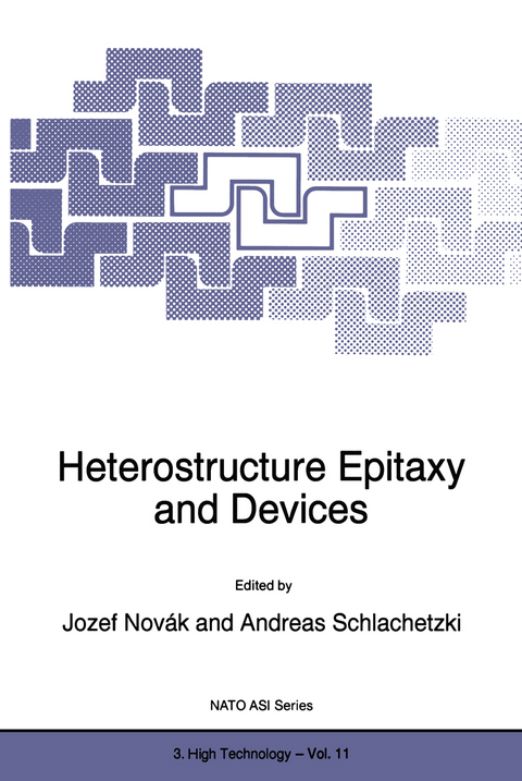
Heterostructure Epitaxy and Devices
Springer (Verlag)
978-0-7923-4018-8 (ISBN)
- Titel z.Zt. nicht lieferbar
- Versandkostenfrei innerhalb Deutschlands
- Auch auf Rechnung
- Verfügbarkeit in der Filiale vor Ort prüfen
- Artikel merken
Section I. Epitaxial growth.- Simulation of III-V layer growth (invited).- Real time monitoring of epitaxial growth (invited).- Influence of carrier gas on AIAs, GaAs and InP MOCVD growth.- LP-MOVPE of III-V semiconductors using highly pure N2 as the carrier gas.- Dependence of properties of LP MOCVD InGaP layers on growth conditions.- Growth of GaN MOCVD layers on GaN single crystals.- Electrical and optical properties of Te-doped GaSb grown by MOVPE.- Computer simulations of epitaxial growth, surface kinetic processes and RHEED intensity oscillations.- Growth and characterization of InP/Ga0.47 In0.53 As deposited by MOMBE.- Investigation of the effect of GaAs buffer layers grown by MBE at different temperatures on the performance of GaAs MESFETs.- Multilayered GaAs VPE structures for micro machining.- Growth of InP and GalnAsP layers by liquid-phase epitaxy using holmium gettering and doping.- Meander type LPE and high temperature stability of elastically strained GalnAsP/InP layers.- Section II. Heterostructures.- Scanning tunneling microscopy characterization of heterostructures.- Microscopic origin of femtosecond spectral hole burning in quantum wells.- Carrier capture due to carrier-carrier interaction in quantum wells.- Optical and theoretical study of GaAs quantum wells embedded in GaAs/AlAs superlattices.- MOCVD growth and characterization of InAs/GaAs superlattices.- Electrical characteristics of epitaxial Al/Al xGa 1-x As /n-Al 0.25Ga 0.75 As heterostructures.- Investigation of a GaAs heterostructure with an AlAs potential barrier by DLTS measurements.- Effect of heterobarriers on the DX center in AlGaAsSb and in GaAlAs.- Mechanical study of the strained InxGa1-x As/GaAs heterostructures.- Hot electrons at semiconductor heterojunctions.- Section III. Composite systems.- III/V-compound semiconductors on silicon (invited).- Crystal growth of column III nitrides by OMVPE (invited).- GaSb dots grown on GaAs surface by MOCVD.- Crystallographic tilting in lattice-mismatched heteroepitaxy: a kinetic approach.- Optimization of MOVPE growth for InGaAs on (00l)Si.- SEM-based characterization techniques for strongly mismatched heteroepitaxy.- Defect characterization of strained InGaAs structures prepared on InP and GaAs.- Influence of the temperature on the morphology and crystal quality of MBE grown InAs/GaAs heterostructures.- Section IV: Characterization.- Study of fundamental growth mechanism by atomic force microscopy (invited).- Characterisation of the epitaxial layers using the lift-off technique (invited).- Many crystal X-ray diffractometry on superlattices (invited).- Quantum magnetotransport in two-dimensional electron gas in InGaAs/InP heterostructures.- Transport properties of MBE GaAs layers grown at 420°C.- Donor neutralisation by hydrogen in S and Se doped GaAs and GaAlAs.- Comparison of photoluminescence spectra of MOCVD and VPE grown GaAs layers.- X-ray diffraction study of MOCVD grown InGaP.- Structural and optical properties of ordered domains in InGaP2 alloys.- Ordering in InGaP prepared by MOCVD.- Ti/Pt/Au ohmic contacts to p-type InGaP.- Comparison of physical properties of bulk crystals and epitaxial layers of GaN.- Section V. Devices.- MOCVD growth of Ga1-xInxAsyP1-y-GaAs quantum structures (invited).- InP-based HBT: principle, design and technology (invited).- Technology and properties of aluminium-free pseudomorphic HEMTs based on InP/InGaAs structures (invited).- Tunneling heterostructure devices (invited).- InGaAs/GaAs pseudomorphic double delta doped HEMTs.- Alpha particle radiation effects in highelectron mobility transistors.- Single versus double current bistability in resonant-tunnelling devices.- Heterostructure lasers based on GaSb and InAs for spectroscopy.- AlAs and InGaP potential barrier photodetector grown on vicinal surfaces.- GaP-based diodes for electrometric applications.- Design of InGaAs/InAlGaAs/InP RCE PIN photodiode.- InP/GalnAs MSM photodetector for simple integration in HEMT circuits.- Nature of internal feedback in the self-electro-optic effect devices.- Optoelectronic integrated circuit A2 B6-insulator- A3B5 with positive feedback.- Characteristics of multiple delta doped GaAs structures.
| Reihe/Serie | NATO Science Partnership Sub-Series: 3 ; 11 |
|---|---|
| Zusatzinfo | 96 Illustrations, black and white; XIII, 323 p. 96 illus. |
| Verlagsort | Dordrecht |
| Sprache | englisch |
| Maße | 160 x 240 mm |
| Themenwelt | Technik ► Elektrotechnik / Energietechnik |
| Technik ► Maschinenbau | |
| ISBN-10 | 0-7923-4018-3 / 0792340183 |
| ISBN-13 | 978-0-7923-4018-8 / 9780792340188 |
| Zustand | Neuware |
| Haben Sie eine Frage zum Produkt? |
aus dem Bereich


