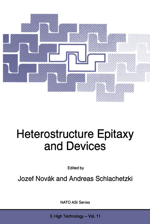
Heterostructure Epitaxy and Devices
Springer (Verlag)
978-94-010-6593-1 (ISBN)
From October 15 to 19, 1995 a Workshop on Hetero- structureEpitaxyandDeviceswasheldatSmoleniceCastlenear Slovakia'scapital Bratislava. The intention ofthisWorkshop was toestablishandstrengthentiesbetweenscientistsoftheformerly Socialist East and Middle-European states with their colleagues fromtheWesterncountries. WiththisaimtheWorkshopfoundthe financialsupportbyNATOwhichtremendouslyhelpedtofacilitate organizingthemeeting That the Workshop was also a scientific success is evidenced by the present volume comprising a selection of the contributed papers. We are confident that the reader of these Proceedings can convincehimselfofthe highqualityofthe work whose results are presented here. We hope that this and the numerousdiscussionsbetweenthe participants ofthe Workshop will promote cooperations among scientists from the countries representedatthemeeting.
It is a pleasure to express our gratitude to NATO and, as representatives ofthe institutions involved in the organization, to Lubomir Malacky (Institute of Electrical Engineering, Slovak Academy of Sciences) and Hergo-Heinrich Wehmann (Institute for Semiconductor Technology, Technical University Braun- schweig) whose dedicated work was most essential for the Workshop. A. Schlachetzki J. Novak November1995 xiii SIMULATIONOFIII-VLAYERGROWTH y. ARIMA DepartmentofPhysics, Gakushuin University 1-5-1 Mejiro, Toshima-ku, Tokyo 171, Japan AND T. IRISAWA ComputerCenter, Gakushuin University 1-5-1 Mejiro, Toshima-ku, Tokyo 171, Japan 1. Introduction Since it was reported [1] that the intensities of RHEED for the growing surface of aGaAs crystal in the process of MBE oscillate with a period correspondingto the completion of a monolayer, this phenomenon has been applied to the thin layer growth of man-made superlattices.
Section I. Epitaxial growth.- Simulation of III-V layer growth (invited).- Real time monitoring of epitaxial growth (invited).- Influence of carrier gas on AIAs, GaAs and InP MOCVD growth.- LP-MOVPE of III-V semiconductors using highly pure N2 as the carrier gas.- Dependence of properties of LP MOCVD InGaP layers on growth conditions.- Growth of GaN MOCVD layers on GaN single crystals.- Electrical and optical properties of Te-doped GaSb grown by MOVPE.- Computer simulations of epitaxial growth, surface kinetic processes and RHEED intensity oscillations.- Growth and characterization of InP/Ga0.47 In0.53 As deposited by MOMBE.- Investigation of the effect of GaAs buffer layers grown by MBE at different temperatures on the performance of GaAs MESFETs.- Multilayered GaAs VPE structures for micro machining.- Growth of InP and GalnAsP layers by liquid-phase epitaxy using holmium gettering and doping.- Meander type LPE and high temperature stability of elastically strained GalnAsP/InP layers.- Section II. Heterostructures.- Scanning tunneling microscopy characterization of heterostructures.- Microscopic origin of femtosecond spectral hole burning in quantum wells.- Carrier capture due to carrier-carrier interaction in quantum wells.- Optical and theoretical study of GaAs quantum wells embedded in GaAs/AlAs superlattices.- MOCVD growth and characterization of InAs/GaAs superlattices.- Electrical characteristics of epitaxial Al/Al xGa 1-x As /n-Al 0.25Ga 0.75 As heterostructures.- Investigation of a GaAs heterostructure with an AlAs potential barrier by DLTS measurements.- Effect of heterobarriers on the DX center in AlGaAsSb and in GaAlAs.- Mechanical study of the strained InxGa1-x As/GaAs heterostructures.- Hot electrons at semiconductor heterojunctions.- Section III. Composite systems.- III/V-compound semiconductors on silicon (invited).- Crystal growth of column III nitrides by OMVPE (invited).- GaSb dots grown on GaAs surface by MOCVD.- Crystallographic tilting in lattice-mismatched heteroepitaxy: a kinetic approach.- Optimization of MOVPE growth for InGaAs on (00l)Si.- SEM-based characterization techniques for strongly mismatched heteroepitaxy.- Defect characterization of strained InGaAs structures prepared on InP and GaAs.- Influence of the temperature on the morphology and crystal quality of MBE grown InAs/GaAs heterostructures.- Section IV: Characterization.- Study of fundamental growth mechanism by atomic force microscopy (invited).- Characterisation of the epitaxial layers using the lift-off technique (invited).- Many crystal X-ray diffractometry on superlattices (invited).- Quantum magnetotransport in two-dimensional electron gas in InGaAs/InP heterostructures.- Transport properties of MBE GaAs layers grown at 420°C.- Donor neutralisation by hydrogen in S and Se doped GaAs and GaAlAs.- Comparison of photoluminescence spectra of MOCVD and VPE grown GaAs layers.- X-ray diffraction study of MOCVD grown InGaP.- Structural and optical properties of ordered domains in InGaP2 alloys.- Ordering in InGaP prepared by MOCVD.- Ti/Pt/Au ohmic contacts to p-type InGaP.- Comparison of physical properties of bulk crystals and epitaxial layers of GaN.- Section V. Devices.- MOCVD growth of Ga1-xInxAsyP1-y-GaAs quantum structures (invited).- InP-based HBT: principle, design and technology (invited).- Technology and properties of aluminium-free pseudomorphic HEMTs based on InP/InGaAs structures (invited).- Tunneling heterostructure devices (invited).- InGaAs/GaAs pseudomorphic double delta doped HEMTs.- Alpha particle radiation effects in highelectron mobility transistors.- Single versus double current bistability in resonant-tunnelling devices.- Heterostructure lasers based on GaSb and InAs for spectroscopy.- AlAs and InGaP potential barrier photodetector grown on vicinal surfaces.- GaP-based diodes for electrometric applications.- Design of InGaAs/InAlGaAs/InP RCE PIN photodiode.- InP/GalnAs MSM photodetector for simple integration in HEMT circuits.- Nature of internal feedback in the self-electro-optic effect devices.- Optoelectronic integrated circuit A2 B6-insulator- A3B5 with positive feedback.- Characteristics of multiple delta doped GaAs structures.
| Reihe/Serie | NATO Science Partnership Sub-Series: 3 ; 11 |
|---|---|
| Zusatzinfo | 96 Illustrations, black and white; XIII, 323 p. 96 illus. |
| Verlagsort | Dordrecht |
| Sprache | englisch |
| Maße | 160 x 240 mm |
| Themenwelt | Technik ► Elektrotechnik / Energietechnik |
| Technik ► Maschinenbau | |
| ISBN-10 | 94-010-6593-4 / 9401065934 |
| ISBN-13 | 978-94-010-6593-1 / 9789401065931 |
| Zustand | Neuware |
| Haben Sie eine Frage zum Produkt? |
aus dem Bereich


