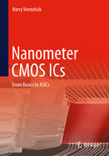
Nanometer CMOS ICs
Springer International Publishing (Verlag)
978-3-319-47595-0 (ISBN)
Harry Veendrick graduated from the Technical University Eindhoven, the Netherlands, in 1977. In the same year he joined Philips Research Laboratories, also in Eindhoven, where he has been involved in the design of memories, gate arrays and complex digital video-signal processors. He holds 30 US and many more European patents in the area of CMOS circuit design, with several other patents pending, and he is the (co-)author of more than 30 publications on robust, high-performance and low-power CMOS IC design. In this respect, he has contributed to many conferences and conference workshops, as reviewer, speaker, invited speaker, panellist, organizer, guest editor and program committee member. In addition, he is the author of MOS ICs (VCH 1992), Deep-Submicron CMOS ICs, from Basics to ASICs (Kluwer Academic Publishers: 1-st edition 1998, 2-nd edition 2000) and Nanometer CMOS ICs, from Basics to ASICs (Springer: 1-st edition June 2008). He is a co-author of Low-Power Electronics Design (CRC Press, 2004). His principle research interests included the design of low-power and high-speed complex digital CMOS circuits, with an emphasis on nanometer-scale physical effects and scaling aspects. From 2002 to 2009 he has been project leader of the Deep-Submicron/Nanometer CMOS Electrical Design Cluster within the research group Mixed-Signal Circuits and Systems at NXP Research, which is the 2006 spin-off of the disentangled former Philips Semiconductors Product and R&D Departments. Complementary to this is his interest in IC technology, which allows him to act as an interface between digital IC design and IC process technology. From 1980 onwards, next to his research activities, he has been actively involved in the training of more than 4500 semiconductor design, test, product, CAD tools and process engineers. In 2002 he received the PhD degree in electronic engineering from the Technical University of Eindhoven, The Netherlands. He was a Research Fellow at Philips Research Laboratories and NXP Research and has been a Visiting Professor to the Department of Electronic and Electrical Engineering of the University of Strathclyde, Glasgow, Scotland, UK. In May 2009 he has left NXP Research and started his own training activity teaching 1-day, 3-day and 5-day courses for different target audiences (NanoCMOS-Training BV).
Basic Principles.- Geometrical-, Physical- and Field-Scaling Impact on MOS Transistor Behavior.- Manufacture of MOS Devices.- CMOS Circuits.- Special Circuits, Devices and Technologies.- Memories.- Very Large Scale Integration (VLSI) and ASICs.- Low Power, a Hot Topic in IC Design.- Robustness of Nanometer CMOS Designs: Signal Integrity, Variability and Reliability.- Testing, Yield, Packaging, Debug and Failure Analysis.- Effects of Scaling on MOS IC Design and Consequences for the Roadmap.
| Erscheinungsdatum | 06.04.2017 |
|---|---|
| Zusatzinfo | XXXVII, 611 p. 445 illus., 271 illus. in color. |
| Verlagsort | Cham |
| Sprache | englisch |
| Maße | 178 x 254 mm |
| Themenwelt | Technik ► Elektrotechnik / Energietechnik |
| Schlagworte | Circuits and Systems • CMOS Integrated Circuit Design • CMOS nanoelectronics • CMOS VLSI design • CMOS VLSI Design textbook • Electronic Circuits and Devices • Electronic devices and materials • Electronics and Microelectronics, Instrumentation • Electronics: circuits and components • Electronics engineering • Engineering • Engineering: general • Nanometer CMOS Integrated Circuits |
| ISBN-10 | 3-319-47595-9 / 3319475959 |
| ISBN-13 | 978-3-319-47595-0 / 9783319475950 |
| Zustand | Neuware |
| Haben Sie eine Frage zum Produkt? |
aus dem Bereich


