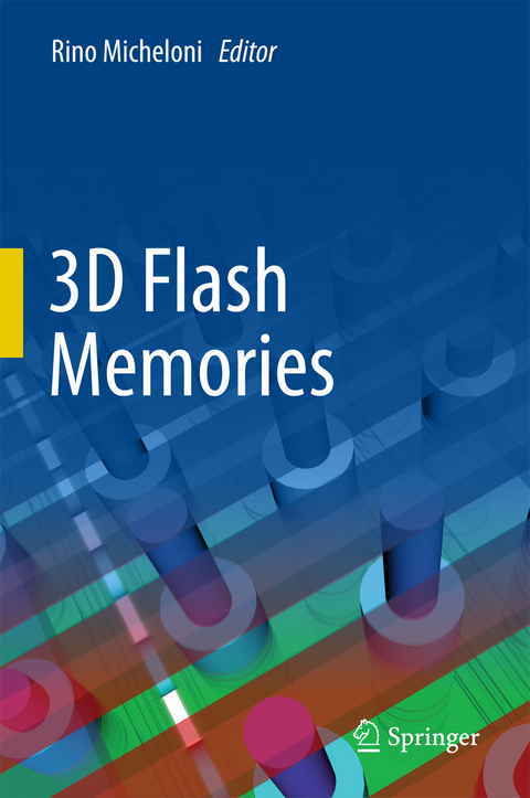
3D Flash Memories (eBook)
XXII, 380 Seiten
Springer Netherland (Verlag)
978-94-017-7512-0 (ISBN)
This book walks the reader through the next step in the evolution of NAND flash memory technology, namely the development of 3D flash memories, in which multiple layers of memory cells are grown within the same piece of silicon. It describes their working principles, device architectures, fabrication techniques and practical implementations, and highlights why 3D flash is a brand new technology.
After reviewing market trends for both NAND and solid state drives (SSDs), the book digs into the details of the flash memory cell itself, covering both floating gate and emerging charge trap technologies. There is a plethora of different materials and vertical integration schemes out there. New memory cells, new materials, new architectures (3D Stacked, BiCS and P-BiCS, 3D FG, 3D VG, 3D advanced architectures); basically, each NAND manufacturer has its own solution. Chapter 3 to chapter 7 offer a broad overview of how 3D can materialize. The 3D wave is impacting emerging memories as well and chapter 8 covers 3D RRAM (resistive RAM) crosspoint arrays. Visualizing 3D structures can be a challenge for the human brain: this is way all these chapters contain a lot of bird's-eye views and cross sections along the 3 axes.
The second part of the book is devoted to other important aspects, such as advanced packaging technology (i.e. TSV in chapter 9) and error correction codes, which have been leveraged to improve flash reliability for decades. Chapter 10 describes the evolution from legacy BCH to the most recent LDPC codes, while chapter 11 deals with some of the most recent advancements in the ECC field. Last but not least, chapter 12 looks at 3D flash memories from a system perspective.
Is 14nm the last step for planar cells? Can 100 layers be integrated within the same piece of silicon? Is 4 bit/cell possible with 3D? Will 3D be reliable enough for enterprise and datacenter applications? These are some of the questions that this book helps answering by providing insights into 3D flash memory design, process technology and applications.
Dr. Rino Micheloni is Fellow at Microsemi Corporation where he currently runs the Non-Volatile Memory Lab in Milan, with special focus on NAND Flash. Prior to joining Microsemi, he was Fellow at PMC-Sierra, working on NAND Flash characterization, LDPC, and NAND Signal Processing as part of the team developing Flash controllers for PCIe SSDs. Before that, he was with IDT (Integrated Device Technology) as Lead Flash Technologist, driving the architecture and design of the BCH engine in the world's 1st PCIe NVMe SSD controller. Early in his career, he led Flash design teams at STMicroelectronics, Hynix, Infineon, and Qimonda; during this time, he developed the industry's first MLC NOR device with embedded ECC technology and the industry's first MLC NAND with embedded BCH.
Rino is IEEE Senior Member, he has co-authored more than 50 publications, and he holds 240 patents worldwide (including 118 US patents). He received the STMicroelectronics Exceptional Patent Award in 2003 and 2004, and the Qimonda IP Award in 2007.
Rino has published the following books with Springer: Inside Solid State Drives (2013), Inside NAND Flash Memories (2010), Error Correction Codes for Non-Volatile Memories (2008), Memories in Wireless Systems (2008), and VLSI-Design of Non-Volatile Memories (2005).
This book walks the reader through the next step in the evolution of NAND flash memory technology, namely the development of 3D flash memories, in which multiple layers of memory cells are grown within the same piece of silicon. It describes their working principles, device architectures, fabrication techniques and practical implementations, and highlights why 3D flash is a brand new technology.After reviewing market trends for both NAND and solid state drives (SSDs), the book digs into the details of the flash memory cell itself, covering both floating gate and emerging charge trap technologies. There is a plethora of different materials and vertical integration schemes out there. New memory cells, new materials, new architectures (3D Stacked, BiCS and P-BiCS, 3D FG, 3D VG, 3D advanced architectures); basically, each NAND manufacturer has its own solution. Chapter 3 to chapter 7 offer a broad overview of how 3D can materialize. The 3D wave is impacting emerging memories as well and chapter 8 covers 3D RRAM (resistive RAM) crosspoint arrays. Visualizing 3D structures can be a challenge for the human brain: this is way all these chapters contain a lot of bird's-eye views and cross sections along the 3 axes.The second part of the book is devoted to other important aspects, such as advanced packaging technology (i.e. TSV in chapter 9) and error correction codes, which have been leveraged to improve flash reliability for decades. Chapter 10 describes the evolution from legacy BCH to the most recent LDPC codes, while chapter 11 deals with some of the most recent advancements in the ECC field. Last but not least, chapter 12 looks at 3D flash memories from a system perspective. Is 14nm the last step for planar cells? Can 100 layers be integrated within the same piece of silicon? Is 4 bit/cell possible with 3D? Will 3D be reliable enough for enterprise and datacenter applications? These are some of the questions that this book helps answering by providing insights into 3D flash memory design, process technology and applications.
Dr. Rino Micheloni is Fellow at Microsemi Corporation where he currently runs the Non-Volatile Memory Lab in Milan, with special focus on NAND Flash. Prior to joining Microsemi, he was Fellow at PMC-Sierra, working on NAND Flash characterization, LDPC, and NAND Signal Processing as part of the team developing Flash controllers for PCIe SSDs. Before that, he was with IDT (Integrated Device Technology) as Lead Flash Technologist, driving the architecture and design of the BCH engine in the world’s 1st PCIe NVMe SSD controller. Early in his career, he led Flash design teams at STMicroelectronics, Hynix, Infineon, and Qimonda; during this time, he developed the industry’s first MLC NOR device with embedded ECC technology and the industry’s first MLC NAND with embedded BCH. Rino is IEEE Senior Member, he has co-authored more than 50 publications, and he holds 240 patents worldwide (including 118 US patents). He received the STMicroelectronics Exceptional Patent Award in 2003 and 2004, and the Qimonda IP Award in 2007. Rino has published the following books with Springer: Inside Solid State Drives (2013), Inside NAND Flash Memories (2010), Error Correction Codes for Non-Volatile Memories (2008), Memories in Wireless Systems (2008), and VLSI-Design of Non-Volatile Memories (2005).
Foreword 6
Preface 9
Acknowledgments 10
Contents 11
About the Editor 13
Introduction 14
NAND Flash Memories: 3D or 5D? 14
1 The Business of NAND 18
1.1 Memory Industry Transformation 18
1.1.1 NAND and Memory Vendor Landscape Consolidation 18
1.1.2 NAND Technology Transitions 20
1.1.3 NAND Usage Model Changes 21
1.2 Solid State Drives 22
1.2.1 Enterprise SSD’s 22
1.2.2 Build-Your-Own (BYO) and Custom SSD’s 27
1.2.2.1 Endurance 29
1.2.2.2 Performance/Power Envelope 29
1.2.2.3 Cost of NAND Flash 30
1.2.3 Economics of SSD Controllers 31
1.2.4 Client SSD’s 33
1.3 NAND Component Technology Evolution: The 3D NAND Transition 33
1.3.1 3D NAND Component Technology 37
1.3.2 3D NAND Output Dominated by TLC 39
1.3.3 Floating Gate Versus Charge Trap 40
1.3.4 Packaging Innovation: TSV NAND 41
1.4 New Memory Technologies on the Horizon 42
1.5 What Do We Look for in the Next 5 Years? 45
2 Reliability of 3D NAND Flash Memories 46
2.1 Introduction 46
2.2 NAND Flash Reliability 47
2.2.1 Endurance 47
2.2.2 Data Retention 48
2.2.3 Erratic Bits and Over-Programming 49
2.3 Architecture Dependent Reliability Issues 50
2.4 2D Charge Trap: Basics 53
2.5 2D Charge Trap: Reliability Issues 54
2.5.1 Endurance Degradation 54
2.5.2 Data Retention 55
2.5.3 Threshold Voltage Shift During Sensing 57
2.6 From 2D to 3D Charge Trap NAND 58
2.7 3D Charge Trap: Reliability Issues 60
2.7.1 Vertical Charge Loss Through Top and Bottom Oxides 61
2.7.2 Lateral Migration Towards Spacers 63
2.7.3 Transient VT Shift 65
2.7.4 Program and Pass Disturbs 66
2.7.5 Vertical Hole Design Limitations 66
2.7.5.1 VT Shift Induced by Stored Electrons During Programming 67
2.7.5.2 VT Shift Induced by Neighboring Cells 68
2.7.5.3 Electric Field in the Tunnel Oxide During Programming 69
2.7.5.4 Design Window of LG and LSPACE 70
2.8 3D CT Versus State-of-the-Art 2D FG 70
2.9 3D-FG Nand 72
2.9.1 DC-SF Interference and Retention Results 73
2.9.2 S-SCG Interference Results 74
2.9.3 S-SCG Performance and Reliability Advantages 74
2.10 3D-CT Versus 3D-FG 76
References 77
3 3D Stacked NAND Flash Memories 80
3.1 Introduction 80
3.2 Floating Gate Cell 84
3.3 NAND Basic Operations 87
3.3.1 Read 87
3.3.2 Program 89
3.3.3 Erase 91
3.4 3D Stacked Architecture 93
3.5 Biasing of 3D Stacked Layers 97
References 99
4 3D Charge Trap NAND Flash Memories 101
4.1 Introduction 101
4.2 BiCS 102
4.3 P-BiCS 111
4.4 VRAT and Z-VRAT 122
4.5 VSAT and A-VSAT 126
4.6 TCAT 131
4.7 V-NAND 137
References 142
5 3D Floating Gate NAND Flash Memories 144
5.1 Introduction 144
5.2 Conventional Floating Gate (C-FG) Flash Cell 144
5.3 Extended Sidewall Control Gate (ESCG) Flash Cell 157
5.4 Dual Control-Gate with Surrounding Floating Gate (DC-SF) Flash Cell 161
5.5 Separated Sidewall Control Gate (S-SCG) Flash Cell 166
5.6 Sidewall Control Pillar (SCP) Flash Cell 170
5.7 Horizontal Channel (HC-FG) Flash Cell 172
5.8 3D FG NAND in the Industry 174
References 179
6 Advanced Architectures for 3D NAND Flash Memories with Vertical Channel 181
6.1 Introduction 181
6.2 Arrays of Conventional Pillars (Holes) 183
6.3 Arrays of Staggered Pillars (Holes) 186
6.4 P-BiCS with Staggered Pillars 192
6.5 Monolithic Even-Odd Rows of Pillars 196
6.6 Staggered Bitline Contacts 200
6.7 Summary 206
References 209
7 3D VG-Type NAND Flash Memories 210
7.1 Introduction 210
7.2 3D NAND Architectures 211
7.3 VG-Type 3D NAND Architecture 215
7.4 Key Architectural Considerations for VG-Type 3D NAND 218
7.5 VG-Type 3D NAND Array Operations 223
7.5.1 Read Operation 224
7.5.2 Program Operation 227
7.5.3 Erase Operation 228
7.6 Disturbs of VG-Type 3D NAND 230
7.7 Conclusions 233
Acknowledgements 233
References 233
8 RRAM Cross-Point Arrays 236
8.1 Introduction of RRAM 236
8.1.1 History and Development 237
8.1.2 Structure and Mechanism of RRAM 238
8.2 3D RRAM 241
8.2.1 3D Architectures 241
8.2.1.1 3D Cross-Point RRAM 242
8.2.1.2 Vertical RRAM 243
8.2.1.3 RRAM Cells in 3D Array 245
8.2.2 Sneak Path Issues in Cross-Point RRAM 247
8.2.2.1 Misreading 247
8.2.2.2 Write Crosstalk 249
8.2.2.3 Solutions 250
8.2.3 Selector Devices 252
8.2.3.1 Diodes 253
8.2.3.2 Tunneling-Based Nonlinear Selectors 253
8.2.3.3 Volatile Switching Selectors 254
8.2.3.4 Mixed Ionic-Electronic Conductors (MIECs) 255
8.2.4 Self-rectifying RRAM 256
8.2.5 Complementary RRAM 258
8.3 Analysis of 3D RRAM Array 260
8.4 Progress of 3D RRAM 261
8.4.1 Intel and Micron 3D XPoint Memory 261
8.4.2 Sandisk and Toshiba 32 Gbit 3D Cross-Point RRAM 262
8.4.3 Crossbar 3D RRAM 264
8.4.4 Others 264
8.5 Challenges and Future Outlook for 3D RRAM 269
References 270
9 3D Multi-chip Integration and Packaging Technology for NAND Flash Memories 274
9.1 3D Multi-chip Integration 274
9.2 Challenges in Nanometer Devices Fabrication 274
9.3 Challenges of On-Chip Interconnections 275
9.4 Heterogeneous Integration Through SiP 276
9.5 Solutions for Size and Cost Reduction 277
9.6 3D Multi-chip SiP Technology Solutions 277
9.6.1 2D, 3D Spatial Configurations of Multi-chip SiP and Derivatives 278
9.6.2 Integration Process of Multi-chip SiP: Die-to-Die, Wafer-to-Wafer and Die-to-Wafer 281
9.6.3 Challenges of 3D Multi-chip SiP 282
9.7 NAND Die Stacking 284
9.8 TSV NAND 288
References 291
10 BCH and LDPC Error Correction Codes for NAND Flash Memories 293
10.1 Introduction 294
10.2 BCH Codes 299
10.2.1 BCH Encoding 300
10.2.2 BCH Decoding 301
10.2.3 Multi-channel BCH 305
10.2.4 Multi-code Rate BCH 308
10.2.5 BCH Detection Properties 311
10.3 Low-Density Parity-Check (LDPC) Codes 314
10.3.1 LDPC Codes and NAND Flash Memories 317
10.3.2 LDPC Code Encoding 319
10.3.3 LDPC Code Decoding 322
10.3.4 QC-LDPC Applied to NAND Flash Memories 328
References 331
11 Advanced Algebraic and Graph-Based ECC Schemes for Modern NVMs 333
11.1 Asymmetric Algebraic ECCs 334
11.1.1 Graded-Bit-Error Correcting Codes 335
11.1.2 Dynamic Thresholds 345
11.2 Non-binary LDPC Codes 348
11.2.1 Binary Trapping/Absorbing Sets 351
11.2.2 Non-binary Absorbing Sets 353
11.2.3 Performance Analysis and Implications 355
11.3 Summary 359
References 359
12 System-Level Considerations on Design of 3D NAND Flash Memories 361
Abstract 361
12.1 Introduction 361
12.2 Background of Solid-State Drive 362
12.3 SSD Performance Improvement Techniques 365
12.3.1 Storage Engine Assisted SSD (SEA-SSD) 365
12.3.2 Logical Block Address (LBA) Scrambled SSD 367
12.3.3 Hybrid M-SCM/3D-NAND Flash SSD 369
12.3.4 All S-SCM SSD 379
12.4 Summary and Conclusion 384
References 386
Index 388
| Erscheint lt. Verlag | 26.5.2016 |
|---|---|
| Zusatzinfo | XXII, 380 p. 396 illus., 304 illus. in color. |
| Verlagsort | Dordrecht |
| Sprache | englisch |
| Themenwelt | Informatik ► Weitere Themen ► Hardware |
| Technik ► Elektrotechnik / Energietechnik | |
| Schlagworte | 3-D Flash Memory Technology • 3-D NAND Flash Memories • 3-D planar charge trap technology • Die Stacking Flash Memory • Floating Gate Cells • Multi-Level Storage • NAND Memory Devices • Silicon Monolithic • Vertical Integration of 3D flash memory |
| ISBN-10 | 94-017-7512-5 / 9401775125 |
| ISBN-13 | 978-94-017-7512-0 / 9789401775120 |
| Haben Sie eine Frage zum Produkt? |
Größe: 28,0 MB
DRM: Digitales Wasserzeichen
Dieses eBook enthält ein digitales Wasserzeichen und ist damit für Sie personalisiert. Bei einer missbräuchlichen Weitergabe des eBooks an Dritte ist eine Rückverfolgung an die Quelle möglich.
Dateiformat: PDF (Portable Document Format)
Mit einem festen Seitenlayout eignet sich die PDF besonders für Fachbücher mit Spalten, Tabellen und Abbildungen. Eine PDF kann auf fast allen Geräten angezeigt werden, ist aber für kleine Displays (Smartphone, eReader) nur eingeschränkt geeignet.
Systemvoraussetzungen:
PC/Mac: Mit einem PC oder Mac können Sie dieses eBook lesen. Sie benötigen dafür einen PDF-Viewer - z.B. den Adobe Reader oder Adobe Digital Editions.
eReader: Dieses eBook kann mit (fast) allen eBook-Readern gelesen werden. Mit dem amazon-Kindle ist es aber nicht kompatibel.
Smartphone/Tablet: Egal ob Apple oder Android, dieses eBook können Sie lesen. Sie benötigen dafür einen PDF-Viewer - z.B. die kostenlose Adobe Digital Editions-App.
Zusätzliches Feature: Online Lesen
Dieses eBook können Sie zusätzlich zum Download auch online im Webbrowser lesen.
Buying eBooks from abroad
For tax law reasons we can sell eBooks just within Germany and Switzerland. Regrettably we cannot fulfill eBook-orders from other countries.
aus dem Bereich


