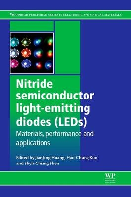
Nitride Semiconductor Light-Emitting Diodes (LEDs)
Woodhead Publishing Ltd (Verlag)
978-0-08-101406-6 (ISBN)
- Titel erscheint in neuer Auflage
- Artikel merken
Part one reviews the fabrication of nitride semiconductor LEDs. Chapters cover molecular beam epitaxy (MBE) growth of nitride semiconductors, modern metalorganic chemical vapor deposition (MOCVD) techniques and the growth of nitride-based materials, and gallium nitride (GaN)-on-sapphire and GaN-on-silicon technologies for LEDs. Nanostructured, non-polar and semi-polar nitride-based LEDs, as well as phosphor-coated nitride LEDs, are also discussed. Part two covers the performance of nitride LEDs, including photonic crystal LEDs, surface plasmon enhanced LEDs, color tuneable LEDs, and LEDs based on quantum wells and quantum dots. Further chapters discuss the development of LED encapsulation technology and the fundamental efficiency droop issues in gallium indium nitride (GaInN) LEDs. Finally, part three highlights applications of nitride LEDs, including liquid crystal display (LCD) backlighting, infrared emitters, and automotive lighting.
Nitride Semiconductor Light-Emitting Diodes (LEDs) is a technical resource for academics, physicists, materials scientists, electrical engineers, and those working in the lighting, consumer electronics, automotive, aviation, and communications sectors.
Prof. JianJang Huang received the B.S. degree in Electrical Engineering (EE) and the M.S. degree in Graduate Institute of Photonics and Optoelectronics (GIPO) from National Taiwan University (NTU), Taipei, Taiwan, in 1994 and 1996, respectively, and the Ph.D. degree in Electrical Engineering from the University of Illinois, Urbana-Champaign, in 2002. He had worked with WJ (Watkins Johnson) Communications in California, as a Staff Scientist from 2002 to 2004. He then came back to Taiwan in 2004 and is currently the professor at NTU EE and GIPO. Prof. Huang has been involved in the development of optoelectronic and electronic devices. He has developed a spin-coating method for nanosphere lithography (NSL) to significantly improve the performance of light emitting diodes (LEDs), solar cells and nanorod devices. His NSL approach has been licensed to several LED companies in Taiwan. He has also fabricated and characterized IGZO TFTs and the corresponding circuits on glass and flexible substrates. In recent years, his group has spent great efforts in realizing cancer cell probes using ZnO nanorods, and high-sensitivity protein sensors based on IGZO TFTs. Prof. Huang is a member of the Phi Tau Phi Scholastic Honor Society. He received “Wu Da-Yu award in 2008, the most prestigious one for young researchers in Taiwan sponsored by National Science Council. And in the same year, he received the award for the most excellent young electrical engineer from the Chinese Institute of Electrical Engineering. He has served in several IPO committees in Taiwan Stock Exchange. He is currently the board director of GCS holdings in Torrance, CA, USA and the conference chair of SPIE, International Conference on Solid-State Lighting. Professor H. C. Kuo received the B.S. degree in Physics from National Taiwan University, Taiwan the M.S. degree in Electrical and computer engineering from Rutgers University in 1995, and the Ph.D. from Center of Compound Semiconductor Microelectronics (CCSM) of University of Illinois- Urbana Champaign in 1998. He has an extensive professional career both in research and industrial research institutions that includes: Research Consultant in Lucent Technologies, Bell Lab (1995-97); Member of Technical Staff in Fiber-optics Division at Agilent Technologies, USA (1999-2001) and Manager of LuxNet Corporation, USA (2001-2002). Since October, 2002 he joined National Chiao Tung University as a faculty member of Institute of Electro-Optical Engineering. Professor Kuo is a member of the IEEE and a recipient of Yang faculty Award from the Foundation for the Advancement of Outstanding Scholarship, he was author and co-author of 70 SCI journal papers and 80 international conference papers. Shyh-Chiang Shen received his B.S. and M.S. degrees, both in electrical engineering, from National Taiwan University in 1993 and 1995, respectively. He received his Ph.D. degree in electrical engineering at the University of Illinois at Urbana-Champaign (UIUC) in 2001. During his graduate study at the University of Illinois, he was involved in the development of low-voltage RF MEMS switches and ion-implanted GaAs MESFET using e-beam direct gate-writing photolithography techniques. Dr. Shen joined Xindium Technologies, Inc. as a senior processing engineer in June 2001. He developed a proprietary high-performance InP SHBT technology for 40Gb/s OEIC applications and InP-based power HBT technology for wireless communications. In August 2004, he joined the HSIC group at the University of Illinois as a postdoctoral research associate to work on exciting research projects. In January 2005, he joined the Georgia Institute of Technology as an Assistant Professor. Dr. Shen holds 7 awarded U.S. patents in the MEMS and microelectronics areas. His current research is focused on wide bandgap semiconductor microelectronics and optoelectronic devices for high-energy-efficiency applications.
Contributor contact details
Woodhead Publishing Series in Electronic and Optical Materials
Dedication
Preface
Part I: Materials and fabrication
1: Molecular beam epitaxy (MBE) growth of nitride semiconductors
Abstract
1.1 Introduction
1.2 Molecular beam epitaxial (MBE) growth techniques
1.3 Plasma-assisted MBE (PAMBE) growth of nitride epilayers and quantum structures
1.4 Nitride nanocolumn (NC) materials
1.5 Nitride nanostructures based on NCs
1.6 Conclusion
2: Modern metal-organic chemical vapor deposition (MOCVD) reactors and growing nitride-based materials
Abstract
2.1 Introduction
2.2 MOCVD systems
2.3 Planetary reactors
2.4 Close-coupled showerhead (CCS) reactors
2.5 In situ monitoring systems and growing nitride-based materials
2.6 Acknowledgements
3: Gallium nitride (GaN) on sapphire substrates for visible LEDs
Abstract
3.1 Introduction
3.2 Sapphire substrates
3.3 Strained heteroepitaxial growth on sapphire substrates
3.4 Epitaxial overgrowth of GaN on sapphire substrates
3.5 GaN growth on non-polar and semi-polar surfaces
3.6 Future trends
4: Gallium nitride (GaN) on silicon substrates for LEDs
Abstract
4.1 Introduction
4.2 An overview of gallium nitride (GaN) on silicon substrates
4.3 Silicon overview
4.4 Challenges for the growth of GaN on silicon substrates
4.5 Buffer-layer strategies
4.6 Device technologies
4.7 Conclusion
5: Phosphors for white LEDs
Abstract
5.1 Introduction
5.2 Optical transitions of Ce3 + and Eu2 +
5.3 Chemical composition of representative nitride and oxynitride phosphors
5.4 Compounds activated by Eu2 +
5.5 Compounds activated by Ce3 +
5.6 Features of the crystal structure of nitride and oxynitride phosphors
5.7 Features of optical transitions of nitride and oxynitride phosphors
5.8 Conclusion and future trends
5.9 Acknowledgements
6: Fabrication of nitride LEDs
Abstract
6.1 Introduction
6.2 GaN-based flip-chip LEDs and flip-chip technology
6.3 GaN FCLEDs with textured micro-pillar arrays
6.4 GaN FCLEDs with a geometric sapphire shaping structure
6.5 GaN thin-film photonic crystal (PC) LEDs
6.6 PC nano-structures and PC LEDs
6.7 Light emission characteristics of GaN PC TFLEDs
6.8 Conclusion
7: Nanostructured LEDs
Abstract
7.1 Introduction
7.2 General mechanisms for growth of gallium nitride (GaN) related materials
7.3 General characterization method
7.4 Top-down technique for nanostructured LEDs
7.5 Bottom-up technique for GaN nanopillar substrates prepared by molecular beam epitaxy
7.6 Conclusion
8: Nonpolar and semipolar LEDs
Abstract
8.1 Motivation: limitations of conventional c-plane LEDs
8.2 Introduction to selected nonpolar and semipolar planes
8.3 Challenges in nonpolar and semipolar epitaxial growth
8.4 Light extraction for nonpolar and semipolar LEDs
Part II: Performance of nitride LEDs
9: Efficiency droop in gallium indium nitride (GaInN)/gallium nitride (GaN) LEDs
Abstract
9.1 Introduction
9.2 Recombination models in LEDs
9.3 Thermal roll-over in gallium indium nitride (GaInN) LEDs
9.4 Auger recombination
9.5 High-level injection and the asymmetry of carrier concentration and mobility
9.6 Non-capture of carriers
9.7 Polarization fields
9.8 Carrier delocalization
9.9 Discussion and comparison of droop mechanisms
9.10 Methods for overcoming droop
10: Photonic crystal nitride LEDs
Abstract
10.1 Introduction
10.2 Photonic crystal (PC) technology
10.3 Improving LED extraction efficiency through PC surface patterning
10.4 PC-enhanced light extraction in P-side up LEDs
10.5 Modelling PC-LEDs
10.6 P-side up PC-LED performance
10.7 PC-enhanced light extraction in N-side up LEDs
10.8 Summary
10.9 Conclusions
11: Surface plasmon enhanced LEDs
Abstract
11.1 Introduction
11.2 Mechanism for plasmon-coupled emission
11.3 Fabrication of plasmon-coupled nanostructures
11.4 Performance and outlook
11.5 Acknowledgements
12: Nitride LEDs based on quantum wells and quantum dots
Abstract
12.1 Light-emitting diodes (LEDS)
12.2 Polarization effects in III-nitride LEDs
12.3 Current status of III-nitride LEDs
12.4 Modern LED designs and enhancements
13: Color tunable LEDs
Abstract
13.1 Introduction
13.2 Initial idea for stacked LEDs
13.3 Second-generation LED stack with inclined sidewalls
13.4 Third-generation tightly integrated chip-stacking approach
13.5 Group-addressable pixelated micro-LED arrays
13.6 Conclusions
14: Reliability of nitride LEDs
Abstract
14.1 Introduction
14.2 Reliability testing of nitride LEDs
14.3 Evaluation of LED degradation
14.4 Degradation mechanisms
14.5 Conclusion
15: Chip packaging: encapsulation of nitride LEDs
Abstract
15.1 Functions of LED chip packaging
15.2 Basic structure of LED packaging modules
15.3 Processes used in LED packaging
15.4 Optical effects of gold wire bonding
15.5 Optical effects of phosphor coating
15.6 Optical effects of freeform lenses
15.7 Thermal design and processing of LED packaging
15.8 Conclusion
Part III: Applications of nitride LEDs
16: White LEDs for lighting applications: the role of standards
Abstract
16.1 General lighting applications
16.2 LED terminology
16.3 Copying traditional lamps?
16.4 Freedom of choice
16.5 Current and future trends
17: Ultraviolet LEDs
Abstract
17.1 Research background of deep ultraviolet (DUV) LEDs
17.2 Growth of low threading dislocation density (TDD) AlN layers on sapphire
17.3 Marked increases in internal quantum efficiency (IQE)
17.4 Aluminum gallium nitride (AlGaN)-based DUV-LEDs fabricated on high-quality aluminum nitride (AlN)
17.5 Increase in electron injection efficiency (EIE) and light extraction efficiency (LEE)
17.6 Conclusions and future trends
18: Infrared emitters made from III-nitride semiconductors
Abstract
18.1 Introduction
18.2 High indium (In) content alloys for infrared emitters
18.3 Rare-earth (RE) doped gallium nitride (GaN) emitters
18.4 III-nitride materials for intersubband (ISB) optoelectronics
18.5 ISB devices
18.6 Conclusions
18.7 Acknowledgements
19: LEDs for liquid crystal display (LCD) backlighting
Abstract
19.1 Introduction
19.2 Types of LED LCD backlighting units (BLUs)
19.3 Technical considerations for optical films and plates
19.4 Requirements for LCD BLUs
19.5 Advantages and history of LED BLUs
19.6 Market trends and technological developments
19.7 Optical design
20: LEDs in automotive lighting
Abstract
20.1 Introduction
20.2 Forward lighting
20.3 Signal lighting
20.4 Human factor issues with LEDs
20.5 Energy and environmental issues
20.6 Future trends
20.7 Sources of further information and advice
20.8 Acknowledgments
Index
| Erscheinungsdatum | 07.07.2016 |
|---|---|
| Reihe/Serie | Woodhead Publishing Series in Electronic and Optical Materials |
| Verlagsort | Cambridge |
| Sprache | englisch |
| Maße | 156 x 234 mm |
| Gewicht | 930 g |
| Themenwelt | Naturwissenschaften ► Physik / Astronomie ► Quantenphysik |
| Technik ► Elektrotechnik / Energietechnik | |
| ISBN-10 | 0-08-101406-6 / 0081014066 |
| ISBN-13 | 978-0-08-101406-6 / 9780081014066 |
| Zustand | Neuware |
| Haben Sie eine Frage zum Produkt? |
aus dem Bereich
