Prof. JianJang Huang received the B.S. degree in Electrical Engineering (EE) and the M.S. degree in Graduate Institute of Photonics and Optoelectronics (GIPO) from National Taiwan University (NTU), Taipei, Taiwan, in 1994 and 1996, respectively, and the Ph.D. degree in Electrical Engineering from the University of Illinois, Urbana-Champaign, in 2002. He had worked with WJ (Watkins Johnson) Communications in California, as a Staff Scientist from 2002 to 2004. He then came back to Taiwan in 2004 and is currently the professor at NTU EE and GIPO.Prof. Huang has been involved in the development of optoelectronic and electronic devices. He has developed a spin-coating method for nanosphere lithography (NSL) to significantly improve the performance of light emitting diodes (LEDs), solar cells and nanorod devices. His NSL approach has been licensed to several LED companies in Taiwan. He has also fabricated and characterized IGZO TFTs and the corresponding circuits on glass and flexible substrates. In recent years, his group has spent great efforts in realizing cancer cell probes using ZnO nanorods, and high-sensitivity protein sensors based on IGZO TFTs.Prof. Huang is a member of the Phi Tau Phi Scholastic Honor Society. He received 'Wu Da-Yu award in 2008, the most prestigious one for young researchers in Taiwan sponsored by National Science Council. And in the same year, he received the award for the most excellent young electrical engineer from the Chinese Institute of Electrical Engineering. He has served in several IPO committees in Taiwan Stock Exchange. He is currently the board director of GCS holdings in Torrance, CA, USA and the conference chair of SPIE, International Conference on Solid-State Lighting."
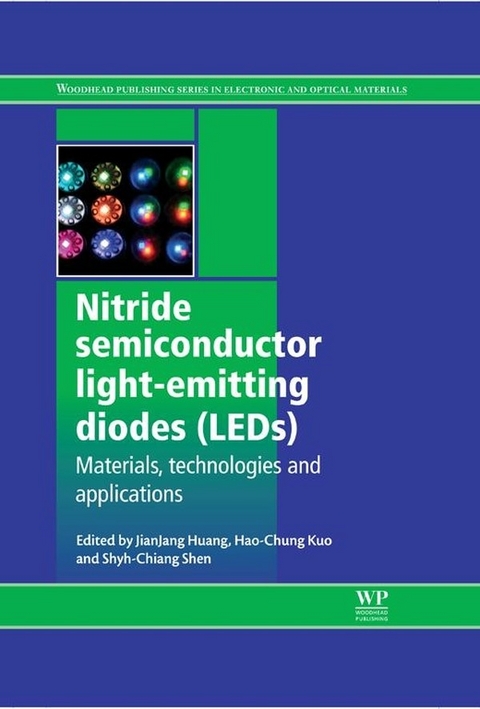
The development of nitride-based light-emitting diodes (LEDs) has led to advancements in high-brightness LED technology for solid-state lighting, handheld electronics, and advanced bioengineering applications. Nitride Semiconductor Light-Emitting Diodes (LEDs) reviews the fabrication, performance, and applications of this technology that encompass the state-of-the-art material and device development, and practical nitride-based LED design considerations. Part one reviews the fabrication of nitride semiconductor LEDs. Chapters cover molecular beam epitaxy (MBE) growth of nitride semiconductors, modern metalorganic chemical vapor deposition (MOCVD) techniques and the growth of nitride-based materials, and gallium nitride (GaN)-on-sapphire and GaN-on-silicon technologies for LEDs. Nanostructured, non-polar and semi-polar nitride-based LEDs, as well as phosphor-coated nitride LEDs, are also discussed. Part two covers the performance of nitride LEDs, including photonic crystal LEDs, surface plasmon enhanced LEDs, color tuneable LEDs, and LEDs based on quantum wells and quantum dots. Further chapters discuss the development of LED encapsulation technology and the fundamental efficiency droop issues in gallium indium nitride (GaInN) LEDs. Finally, part three highlights applications of nitride LEDs, including liquid crystal display (LCD) backlighting, infrared emitters, and automotive lighting. Nitride Semiconductor Light-Emitting Diodes (LEDs) is a technical resource for academics, physicists, materials scientists, electrical engineers, and those working in the lighting, consumer electronics, automotive, aviation, and communications sectors. - Reviews fabrication, performance, and applications of this technology that encompass the state-of-the-art material and device development, and practical nitride-based LED design considerations- Covers the performance of nitride LEDs, including photonic crystal LEDs, surface plasmon enhanced LEDs, color tuneable LEDs, and LEDs based on quantum wells and quantum dots- Highlights applications of nitride LEDs, including liquid crystal display (LCD) backlighting, infra-red emitters, and automotive lighting
Cover
1
Nitride semiconductor light-emitting diodes(LEDs): Materials, technologies and applications
4
Copyright 5
Contents 6
Contributor contact details 14
Woodhead Publishing Series in Electronic and Optical Materials 18
Dedication 23
Preface 24
Part I:
28
1:
30
1.1 Introduction 30
1.2 Molecular beam epitaxial (MBE) growth techniques 31
1.3 Plasmaassisted MBE (PAMBE) growth of nitride epilayers and quantum structures 32
1.4 Nitride nanocolumn (NC) materials 39
1.5 Nitride nanostructures based on NCs 44
1.6 Conclusion 48
1.7 References 48
2:
54
2.1 Introduction 54
2.2 MOCVD systems 55
2.3 Planetary reactors 62
2.4 Closecoupled showerhead (CCS) reactors 72
2.5 In situ monitoring systems and growing nitridebased materials
81
2.6 Acknowledgements 92
2.7 References 92
3:
93
3.1 Introduction 93
3.2 Sapphire substrates 96
3.3 Strained heteroepitaxial growth on sapphire substrates 104
3.4 Epitaxial overgrowth of GaN on sapphire substrates 108
3.5 GaN growth on nonpolar and semipolar surfaces 113
3.6 Future trends 115
3.7 References 116
4:
126
4.1 Introduction 126
4.2 An overview of gallium nitride (GaN) on silicon substrates 127
4.3 Silicon overview 128
4.4 Challenges for the growth of GaN on silicon substrates 131
4.5 Bufferlayer strategies 132
4.6 Device technologies 140
4.7 Conclusion 166
4.8 References 166
5:
171
5.1 Introduction 171
5.2 Optical transitions of Ce and Eu
173
5.3 Chemical composition of representative nitride and oxynitride phosphors 176
5.4 Compounds activated by Eu 177
5.5 Compounds activated by Ce 192
5.6 Features of the crystal structure of nitride and oxynitride phosphors 195
5.7 Features of optical transitions of nitride and oxynitride phosphors 198
5.8 Conclusion and future trends 202
5.9 Acknowledgements 203
5.10 References 203
6:
208
6.1 Introduction 208
6.2 GaN-based fl ipchip LEDs and fl ipchip technology 210
6.3 GaN FCLEDs with textured micropillar arrays 212
6.4 GaN FCLEDs with a geometric sapphire shaping structure 218
6.5 GaN thinfi lm photonic crystal (PC) LEDs 225
6.6 PC nanostructures and PC LEDs 227
6.7 Light emission characteristics of GaN PC TFLEDs 232
6.8 Conclusion 238
6.9 References 239
7: Nanostructured LEDs
243
7.1 Introduction 243
7.2 General mechanisms for growth of gallium nitride (GaN) related materials 245
7.3 General characterization method 250
7.4 Topdown technique for nanostructured LEDs 252
7.5 Bottomup technique for GaN nanopillar substrates prepared by molecular beam epitaxy 267
7.6 Conclusion 272
7.7 References 272
8:
277
8.1 Motivation: limitations of conventional cplane LEDs 277
8.2 Introduction to selected nonpolar and semipolar planes 282
8.3 Challenges in nonpolar and semipolar epitaxial growth 290
8.4 Light extraction for nonpolar and semipolar LEDs 294
8.5 References 297
Part II:
304
9: Efficiency droop in gallium indium nitride (GaInN)/gallium nitride (GaN) LEDs
306
9.1 Introduction 306
9.2 Recombination models in LEDs 308
9.3 Thermal rollover in gallium indium nitride (GaInN) LEDs 309
9.4 Auger recombination 311
9.5 Highlevel injection and the asymmetry of carrier concentration and mobility 313
9.6 Noncapture of carriers 317
9.7 Polarization fi elds 318
9.8 Carrier delocalization 318
9.9 Discussion and comparison of droop mechanisms 320
9.10 Methods for overcoming droop 321
9.11 References 325
10:
328
10.1 Introduction 328
10.2 Photonic crystal (PC) technology 337
10.3 Improving LED extraction effi ciency through PC surface patterning 345
10.4 PC-enhanced light extraction in P-side up LEDs 349
10.5 Modelling PC-LEDs 353
10.6 P-side up PC-LED performance 382
10.7 PC-enhanced light extraction in N-side up LEDs 389
10.8 Summary 397
10.9 Conclusions 399
10.10 References 400
11:
402
11.1 Introduction 402
11.2 Mechanism for plasmoncoupled emission 403
11.3 Fabrication of plasmoncoupled nanostructures 405
11.4 Performance and outlook 410
11.5 Acknowledgements 412
11.6 References 412
12:
415
12.1 Lightemitting diodes (LEDS) 415
12.2 Polarization effects in III-nitride LEDs 426
12.3 Current status of III-nitride LEDs 437
12.4 Modern LED designs and enhancements 446
12.5 References 447
13:
456
13.1 Introduction 456
13.2 Initial idea for stacked LEDs 457
13.3 Secondgeneration LED stack with inclined sidewalls 459
13.4 Thirdgeneration tightly integrated chipstacking approach 464
13.5 Groupaddressable pixelated micro-LED arrays 470
13.6 Conclusions 473
13.7 References 474
14:
475
14.1 Introduction 475
14.2 Reliability testing of nitride LEDs 475
14.3 Evaluation of LED degradation 478
14.4 Degradation mechanisms 481
14.5 Conclusion 486
14.6 References 487
15:
488
15.1 Functions of LED chip packaging 488
15.2 Basic structure of LED packaging modules 493
15.3 Processes used in LED packaging 496
15.4 Optical effects of gold wire bonding 500
15.5 Optical effects of phosphor coating 503
15.6 Optical effects of freeform lenses 510
15.7 Thermal design and processing of LED packaging 515
15.8 Conclusion 523
15.9 References 523
Part III:
530
16:
532
16.1 General lighting applications 532
16.2 LED terminology 534
16.3 Copying traditional lamps? 537
16.4 Freedom of choice 538
16.5 Current and future trends 541
16.6 References 542
17: Ultraviolet LEDs
544
17.1 Research background of deep ultraviolet (DUV) LEDs 544
17.2 Growth of low threading dislocation density (TDD) AlN layers on sapphire 549
17.3 Marked increases in internal quantum effi ciency (IQE) 554
17.4 Aluminum gallium nitride (AlGaN)-based DUV-LEDs fabricated on highquality aluminum nitride (AlN) 560
17.5 Increase in electron injection effi ciency (EIE) and light extraction effi ciency (LEE) 568
17.6 Conclusions and future trends 575
17.7 References 577
18:
580
18.1 Introduction 580
18.2 High indium (In) content alloys for infrared emitters 581
18.3 Rareearth (RE) doped gallium nitride (GaN) emitters 583
18.4 III-nitride materials for intersubband (ISB) optoelectronics 585
18.5 ISB devices 596
18.6 Conclusions 603
18.7 Acknowledgements 604
18.8 References 604
19:
613
19.1 Introduction 613
19.2 Types of LED LCD backlighting units (BLUs) 614
19.3 Technical considerations for optical fi lms and plates 618
19.4 Requirements for LCD BLUs 619
19.5 Advantages and history of LED BLUs 621
19.6 Market trends and technological developments 624
19.7 Optical design 630
19.8 References 640
20:
642
20.1 Introduction 642
20.2 Forward lighting 642
20.3 Signal lighting 646
20.4 Human factor issues with LEDs 646
20.5 Energy and environmental issues 650
20.6 Future trends 650
20.7 Sources of further information and advice 651
20.8 Acknowledgments 651
20.9 References 651
Index 654
Woodhead Publishing Series in Electronic and Optical Materials
1 Circuit analysis
J. E. Whitehouse
2 Signal processing in electronic communications: For engineers and mathematicians
M. J. Chapman, D. P. Goodall and N. C. Steele
3 Pattern recognition and image processing
D. Luo
4 Digital filters and signal processing in electronic engineering: Theory, applications, architecture, code
S. M. Bozic and R. J. Chance
5 Cable engineering for local area networks
B. J. Elliott
6 Designing a structured cabling system to ISO 11801: Cross-referenced to European CENELEC and American Standards
Second edition
B. J. Elliott
7 Microscopy techniques for materials science
A. Clarke and C. Eberhardt
8 Materials for energy conversion devices
Edited by C. C. Sorrell, J. Nowotny and S. Sugihara
9 Digital image processing: Mathematical and computational methods Second edition
J. M. Blackledge
10 Nanolithography and patterning techniques in microelectronics
Edited by D. Bucknall
11 Digital signal processing: Mathematical and computational methods, software development and applications
Second edition
J. M. Blackledge
12 Handbook of advanced dielectric, piezoelectric and ferroelectric materials: Synthesis, properties and applications
Edited by Z.-G. Ye
13 Materials for fuel cells
Edited by M. Gasik
14 Solid-state hydrogen storage: Materials and chemistry
Edited by G. Walker
15 Laser cooling of solids
S. V. Petrushkin and V. V. Samartsev
16 Polymer electrolytes: Fundamentals and applications
Edited by C. A. C. Sequeira and D. A. F. Santos
17 Advanced piezoelectric materials: Science and technology
Edited by K. Uchino
18 Optical switches: Materials and design
Edited by S. J. Chua and B. Li
19 Advanced adhesives in electronics: Materials, properties and applications
Edited by M. O. Alam and C. Bailey
20 Thin film growth: Physics, materials science and applications
Edited by Z. Cao
21 Electromigration in thin films and electronic devices: Materials and reliability
Edited by C.-U. Kim
22 In situ characterization of thin film growth
Edited by G. Koster and G. Rijnders
23 Silicon-germanium (SiGe) nanostructures: Production, properties and applications in electronics
Edited by Y. Shiraki and N. Usami
24 High-temperature superconductors
Edited by X. G. Qiu
25 Introduction to the physics of nanoelectronics
S. G. Tan and M. B. A. Jalil
26 Printed films: Materials science and applications in sensors, electronics and photonics
Edited by M. Prudenziati and J. Hormadaly
27 Laser growth and processing of photonic devices
Edited by N. A. Vainos
28 Quantum optics with semiconductor nanostructures
Edited by F. Jahnke
29 Ultrasonic transducers: Materials and design for sensors, actuators and medical applications
Edited by K. Nakamura
30 Waste electrical and electronic equipment (WEEE) handbook
Edited by V. Goodship and A. Stevels
31 Applications of ATILA FEM software to smart materials: Case studies in designing devices
Edited by K. Uchino and J.-C. Debus
32 MEMS for automotive and aerospace applications
Edited by M. Kraft and N. M. White
33 Semiconductor lasers: Fundamentals and applications
Edited by A. Baranov and E. Tournie
34 Handbook of terahertz technology for imaging, sensing and communications
Edited by D. Saeedkia
35 Handbook of solid-state lasers: Materials, systems and applications
Edited by B. Denker and E. Shklovsky
36 Organic light-emitting diodes (OLEDs): Materials, devices and applications
Edited by A. Buckley
37 Lasers for medical applications: Diagnostics, therapy and surgery
Edited by H. Jelínková
38 Semiconductor gas sensors
Edited by R. Jaaniso and O. K. Tan
39 Handbook of organic materials for optical and (opto)electronic devices: Properties and applications
Edited by O. Ostroverkhova
40 Metallic films for electronic, optical and magnetic applications: Structure, processing and properties
Edited by K. Barmak and K. Coffey
41 Handbook of laser welding technologies
Edited by S. Katayama
42 Nanolithography: The art of fabricating nanoelectronic and nanophotonic devices and systems
Edited by M. Feldman
43 Laser spectroscopy for sensing: Fundamentals, techniques and applications
Edited by M. Baudelet
44 Chalcogenide glasses: Preparation, properties and applications
Edited by J.-L. Adam and X. Zhang
45 Handbook of MEMS for wireless and mobile applications
Edited by D. Uttamchandani
46 Subsea optics and imaging
Edited by J. Watson and O. Zielinski
47 Carbon nanotubes and graphene for photonic applications
Edited by S. Yamashita, Y. Saito and J. H. Choi
48 Optical biomimetics: Materials and applications
Edited by M. Large
49 Optical thin films and coatings
Edited by A. Piegari and F. Flory
50 Computer design of diffractive optics
Edited by V. A. Soifer
51 Smart sensors and MEMS: Intelligent devices and microsystems for industrial applications
Edited by S. Nihtianov and A. Luque
52 Fundamentals of femtosecond...
| Erscheint lt. Verlag | 14.2.2014 |
|---|---|
| Sprache | englisch |
| Themenwelt | Naturwissenschaften ► Physik / Astronomie ► Quantenphysik |
| Technik ► Elektrotechnik / Energietechnik | |
| Technik ► Maschinenbau | |
| ISBN-10 | 0-85709-930-2 / 0857099302 |
| ISBN-13 | 978-0-85709-930-3 / 9780857099303 |
| Haben Sie eine Frage zum Produkt? |
Größe: 63,9 MB
Kopierschutz: Adobe-DRM
Adobe-DRM ist ein Kopierschutz, der das eBook vor Mißbrauch schützen soll. Dabei wird das eBook bereits beim Download auf Ihre persönliche Adobe-ID autorisiert. Lesen können Sie das eBook dann nur auf den Geräten, welche ebenfalls auf Ihre Adobe-ID registriert sind.
Details zum Adobe-DRM
Dateiformat: PDF (Portable Document Format)
Mit einem festen Seitenlayout eignet sich die PDF besonders für Fachbücher mit Spalten, Tabellen und Abbildungen. Eine PDF kann auf fast allen Geräten angezeigt werden, ist aber für kleine Displays (Smartphone, eReader) nur eingeschränkt geeignet.
Systemvoraussetzungen:
PC/Mac: Mit einem PC oder Mac können Sie dieses eBook lesen. Sie benötigen eine
eReader: Dieses eBook kann mit (fast) allen eBook-Readern gelesen werden. Mit dem amazon-Kindle ist es aber nicht kompatibel.
Smartphone/Tablet: Egal ob Apple oder Android, dieses eBook können Sie lesen. Sie benötigen eine
Geräteliste und zusätzliche Hinweise
Buying eBooks from abroad
For tax law reasons we can sell eBooks just within Germany and Switzerland. Regrettably we cannot fulfill eBook-orders from other countries.
Größe: 20,1 MB
Kopierschutz: Adobe-DRM
Adobe-DRM ist ein Kopierschutz, der das eBook vor Mißbrauch schützen soll. Dabei wird das eBook bereits beim Download auf Ihre persönliche Adobe-ID autorisiert. Lesen können Sie das eBook dann nur auf den Geräten, welche ebenfalls auf Ihre Adobe-ID registriert sind.
Details zum Adobe-DRM
Dateiformat: EPUB (Electronic Publication)
EPUB ist ein offener Standard für eBooks und eignet sich besonders zur Darstellung von Belletristik und Sachbüchern. Der Fließtext wird dynamisch an die Display- und Schriftgröße angepasst. Auch für mobile Lesegeräte ist EPUB daher gut geeignet.
Systemvoraussetzungen:
PC/Mac: Mit einem PC oder Mac können Sie dieses eBook lesen. Sie benötigen eine
eReader: Dieses eBook kann mit (fast) allen eBook-Readern gelesen werden. Mit dem amazon-Kindle ist es aber nicht kompatibel.
Smartphone/Tablet: Egal ob Apple oder Android, dieses eBook können Sie lesen. Sie benötigen eine
Geräteliste und zusätzliche Hinweise
Buying eBooks from abroad
For tax law reasons we can sell eBooks just within Germany and Switzerland. Regrettably we cannot fulfill eBook-orders from other countries.
aus dem Bereich


