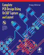
Complete PCB Design Using OrCad Capture and Layout
Seiten
2007
Newnes (an imprint of Butterworth-Heinemann Ltd ) (Verlag)
978-0-7506-8214-5 (ISBN)
Newnes (an imprint of Butterworth-Heinemann Ltd ) (Verlag)
978-0-7506-8214-5 (ISBN)
- Titel erscheint in neuer Auflage
- Artikel merken
Zu diesem Artikel existiert eine Nachauflage
Provides instruction on how to use the OrCAD design suite to design and manufacture printed circuit boards. This book shows the reader how to design a PCB using OrCAD Capture and OrCAD Layout. It also shows the reader how to add PSpice simulation capabilities to the design, and how to develop custom schematic parts, footprints and PSpice models.
Complete PCB Design Using OrCad Capture and Layout provides instruction on how to use the OrCAD design suite to design and manufacture printed circuit boards. The book is written for both students and practicing engineers who need a quick tutorial on how to use the software and who need in-depth knowledge of the capabilities and limitations of the software package. There are two goals the book aims to reach:
The primary goal is to show the reader how to design a PCB using OrCAD Capture and OrCAD Layout. Capture is used to build the schematic diagram of the circuit, and Layout is used to design the circuit board so that it can be manufactured.
The secondary goal is to show the reader how to add PSpice simulation capabilities to the design, and how to develop custom schematic parts, footprints and PSpice models. Often times separate designs are produced for documentation, simulation and board fabrication. This book shows how to perform all three functions from the same schematic design. This approach saves time and money and ensures continuity between the design and the manufactured product.
Kraig Mitzner is a consultant in Silverdale, WA, USA
Chapter 1 Introduction to CAD and PCB fabricationChapter 2 Introduction to the PCB Design flow by example Chapter 3 Project Structures and the Layout ToolsetChapter 4 Introduction to Industry StandardsChapter 5 PCB Design for manufacturabilityChapter 6 PCB Design for signal integrityChapter 7 Making and Editing Capture PartsChapter 8 Making and editing Layout footprintsChapter 9 PCB Design ExamplesChapter 10 Post processing and board fabricationChapter 11 Additional Tools
| Erscheint lt. Verlag | 3.5.2007 |
|---|---|
| Verlagsort | Oxford |
| Sprache | englisch |
| Maße | 191 x 235 mm |
| Gewicht | 1180 g |
| Themenwelt | Technik ► Elektrotechnik / Energietechnik |
| ISBN-10 | 0-7506-8214-0 / 0750682140 |
| ISBN-13 | 978-0-7506-8214-5 / 9780750682145 |
| Zustand | Neuware |
| Haben Sie eine Frage zum Produkt? |
Mehr entdecken
aus dem Bereich
aus dem Bereich
Kolbenmaschinen - Strömungsmaschinen - Kraftwerke
Buch | Hardcover (2023)
Hanser (Verlag)
49,99 €


