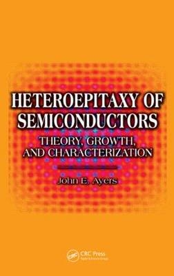
Heteroepitaxy of Semiconductors
Crc Press Inc (Verlag)
978-0-8493-7195-0 (ISBN)
- Titel erscheint in neuer Auflage
- Artikel merken
Heteroepitaxy has evolved rapidly in recent years. With each new wave of material/substrate combinations, our understanding of how to control crystal growth becomes more refined. Most books on the subject focus on a specific material or material family, narrowly explaining the processes and techniques appropriate for each. Surveying the principles common to all types of semiconductor materials, Heteroepitaxy of Semiconductors: Theory, Growth, and Characterization is the first comprehensive, fundamental introduction to the field. This book reflects our current understanding of nucleation, growth modes, relaxation of strained layers, and dislocation dynamics without emphasizing any particular material. Following an overview of the properties of semiconductors, the author introduces the important heteroepitaxial growth methods and provides a survey of semiconductor crystal surfaces, their structures, and nucleation. With this foundation, the book provides in-depth descriptions of mismatched heteroepitaxy and lattice strain relaxation, various characterization tools used to monitor and evaluate the growth process, and finally, defect engineering approaches. Numerous examples highlight the concepts while extensive micrographs, schematics of experimental setups, and graphs illustrate the discussion.
Serving as a solid starting point for this rapidly evolving area, Heteroepitaxy of Semiconductors: Theory, Growth, and Characterization makes the principles of heteroepitaxy easily accessible to anyone preparing to enter the field.
University of Connecticut, Storrs, USA
Introduction
Properties of Semiconductors
Introduction
Crystallographic Properties
Lattice Constants and Thermal Expansion Coefficients
Elastic Properties
Surface Free Energy
Dislocations
Planar Defects
Problems
References
Heteroepitaxial Growth
Introduction
Vapor Phase Epitaxy (VPE)
Molecular Beam Epitaxy (MBE)
Silicon, Germanium, and Si1-xGex Alloys
Silicon Carbide
III-Arsenides, III-Phosphides, and III-Antimonides
III-Nitrides
II-VI Semiconductors
Conclusion
Problems
References
Surface and Chemical Considerations in Heteroepitaxy
Introduction
Surface Reconstructions
Nucleation
Growth Modes
Nucleation Layers
Surfactants in Heteroepitaxy
Quantum Dots and Self-Assembly
Problems
References
Mismatched Heteroepitaxial Growth and Strain Relaxation
Introduction
Pseudomorphic Growth and the Critical Layer Thickness
Dislocation Sources
Interactions between Misfit Dislocations
Lattice Relaxation Mechanisms
Quantitative Models for Lattice Relaxation
Lattice Relaxation on Vicinal Substrates: Crystallographic Tilting of Heteroepitaxial Layers
Lattice Relaxation in Graded Layers
Lattice Relaxation in Superlattices and Multilayer Structures
Dislocation Coalescence, Annihilation, and Removal in Relaxed Heteroepitaxial Layers
Thermal Strain
Cracking in Thick Films
Problems
References
Characterization of Heteroepitaxial Layers
Introduction
X-Ray Diffraction
Electron Diffraction
Microscopy
Crystallographic Etching Techniques
Photoluminescence
Growth Rate and Layer Thickness
Composition and Strain
Determination of Critical Layer Thickness
Crystal Orientation
Defect Types and Densities
Multilayered Structures and Superlattices
Growth Mode
Problems
References
Defect Engineering in Heteroepitaxial Layers
Introduction
Buffer Layer Approaches
Reduced Area Growth Using Patterned Substrates
Patterning and Annealing
Epitaxial Lateral Overgrowth (ELO)
Pendeo-Epitaxy
Nanoheteroepitaxy
Planar Compliant Substrates
Free-Standing Semiconductor Films
Conclusion
Problems
References
Appendix A: Bandgap Engineering Diagrams
Appendix B: Lattice Constants and Coefficients of Thermal Expansion
Appendix C: Elastic Constants
Appendix D: Critical Layer Thickness
Appendix E: Crystallographic Etches
Appendix F: Tables for X-Ray Diffraction Index
| Erscheint lt. Verlag | 31.1.2007 |
|---|---|
| Zusatzinfo | 500 equations; 39 Tables, black and white; 194 Illustrations, black and white |
| Verlagsort | Bosa Roca |
| Sprache | englisch |
| Maße | 156 x 235 mm |
| Gewicht | 771 g |
| Themenwelt | Naturwissenschaften ► Physik / Astronomie ► Elektrodynamik |
| Technik ► Elektrotechnik / Energietechnik | |
| ISBN-10 | 0-8493-7195-3 / 0849371953 |
| ISBN-13 | 978-0-8493-7195-0 / 9780849371950 |
| Zustand | Neuware |
| Haben Sie eine Frage zum Produkt? |
aus dem Bereich


