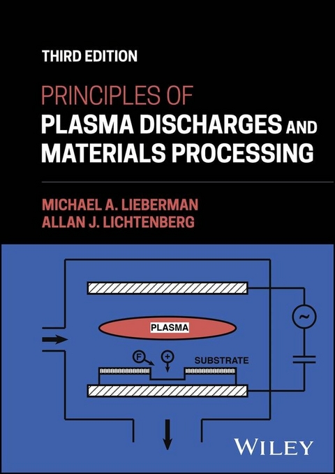
Principles of Plasma Discharges and Materials Processing (eBook)
832 Seiten
Wiley (Verlag)
978-1-394-24539-0 (ISBN)
A new edition of this industry classic on the principles of plasma processing
Plasma-based technology and materials processes have been central to the revolution of the last half-century in micro- and nano-electronics. From anisotropic plasma etching on microprocessors, memory, and analog chips, to plasma deposition for creating solar panels and flat-panel displays, plasma-based materials processes have reached huge areas of technology. As key technologies scale down in size from the nano- to the atomic level, further developments in plasma materials processing will only become more essential.
Principles of Plasma Discharges and Materials Processing is the foundational introduction to the subject. It offers detailed information and procedures for designing plasma-based equipment and analyzing plasma-based processes, with an emphasis on the abiding fundamentals. Now fully updated to reflect the latest research and data, it promises to continue as an indispensable resource for graduate students and industry professionals in a myriad of technological fields.
Readers of the third edition of Principles of Plasma Discharges and Materials Processing will also find:
- Extensive figures and tables to facilitate understanding
- A new chapter covering the recent development of processes involving high-pressure capacitive discharges
- New subsections on discharge and processing chemistry, physics, and diagnostics
Principles of Plasma Discharges and Materials Processing is ideal for professionals and process engineers in the field of plasma-assisted materials processing with experience in the field of science or engineering. It is the premiere world-wide basic text for graduate courses in the field.
Michael A. Lieberman, PhD, is Professor of the Graduate School, Department of Electrical Engineering and Computer Sciences, University of California, Berkeley.
Allan J. Lichtenberg, PhD, was Emeritus Professor of the Department of Electrical Engineering and Computer Sciences, University of California, Berkeley.
A new edition of this industry classic on the principles of plasma processing Plasma-based technology and materials processes have been central to the revolution of the last half-century in micro- and nano-electronics. From anisotropic plasma etching on microprocessors, memory, and analog chips, to plasma deposition for creating solar panels and flat-panel displays, plasma-based materials processes have reached huge areas of technology. As key technologies scale down in size from the nano- to the atomic level, further developments in plasma materials processing will only become more essential. Principles of Plasma Discharges and Materials Processing is the foundational introduction to the subject. It offers detailed information and procedures for designing plasma-based equipment and analyzing plasma-based processes, with an emphasis on the abiding fundamentals. Now fully updated to reflect the latest research and data, it promises to continue as an indispensable resource for graduate students and industry professionals in a myriad of technological fields. Readers of the third edition of Principles of Plasma Discharges and Materials Processing will also find: Extensive figures and tables to facilitate understanding A new chapter covering the recent development of processes involving high-pressure capacitive discharges New subsections on discharge and processing chemistry, physics, and diagnostics Principles of Plasma Discharges and Materials Processing is ideal for professionals and process engineers in the field of plasma-assisted materials processing with experience in the field of science or engineering. It is the premiere world-wide basic text for graduate courses in the field.
List of Figures
- Figure 1.1 High aspect ratio anisotropic etches, showing the extraordinary capabilities of plasma processing; such etched features are used for device isolation, charge storage capacitors, channel holes, and many other purposes in integrated circuits: trench etch (0.2 m wide by 4 m deep) in single-crystal silicon, circa 2004; set of channel holes (each approximately 0.1 m in diameter by 7.5 m deep) etched into a stacked set of dielectric layers, circa 2023. Source: (a) M. A. Lieberman (Book Author). (b) Courtesy of Lam Research Corporation
- Figure 1.2 Deposition and pattern transfer in manufacturing an integrated circuit: metal deposition; photoresist deposition; optical exposure through a pattern; photoresist development; anisotropic plasma etch; remaining photoresist removal
- Figure 1.3 Plasma etching in integrated circuit manufacture: example of isotropic etch; sidewall etching of the resist mask leads to a loss of anisotropy in film etch; illustrating the role of bombarding ions in anisotropic etch; illustrating the role of sidewall passivating films in anisotropic etch
- Figure 1.4 Experimental demonstration of ion-enhanced plasma etching. Source: Adapted from Coburn and Winters (1979)
- Figure 1.5 Illustrating ion implantation of an irregular object: in a conventional ion beam implanter, the beam is electrically scanned and the target object is mechanically rotated and tilted to achieve uniform implantation; in plasma-immersion ion implantation (PIII), the target is immersed in a plasma, and ions from the plasma are implanted with a relatively uniform spatial distribution
- Figure 1.6 Schematic view of a plasma and a discharge
- Figure 1.7 Energy coupling between electrons and heavy particles in a low-pressure plasma
- Figure 1.8 Space and laboratory plasmas on a versus diagram (Source: Book (1987)/Naval Research Laboratory); the electron Debye length is defined in Section 2.4
- Figure 1.9 Densities and energies for various species in a low-pressure capacitive rf discharge
- Figure 1.10 Electron energy distribution function in a weakly ionized discharge
- Figure 1.11 The formation of plasma sheaths: initial ion and electron densities and potential; densities, electric field, and potential after the formation of the sheath
- Figure 1.12 PIC simulation of positive ion sheath formation: – electron phase space, with horizontal scale in meters; electron density ; electric field ; potential ; electron number versus time in seconds; right hand potential versus time
- Figure 1.13 Typical multi-wafer capacitive rf discharge in plane-parallel geometry, used for anisotropic etching. Source: Lieberman and Gottscho (1994)/with permission of Elsevier
- Figure 1.14 The physical model of an rf diode. Source: Lieberman and Gottscho (1994)/with permission of Elsevier
- Figure 1.15 Some modern capacitive discharges are used for etching and deposition; single frequency, dual frequency, and magnetically enhanced
- Figure 1.16 Some non-capacitive, high-density discharges used for etching and deposition; planar inductive; electron cyclotron resonance; helicon
- Figure 1.17 A dc planar magnetron discharge, used for thin film deposition
- Figure 1.18 The central problem of discharge analysis
- Figure 2.1 Kirchhoff’s circuit laws: the total current flowing across a nonuniform one-dimensional discharge is independent of ; the sum of the currents entering a node is zero ( ); the sum of voltages around a loop is zero ()
- Figure 2.2 PIC simulation of ion loss in a plasma containing ions only: () – ion phase space, showing the ion acceleration trajectories; () number of ion sheets versus , with the steps indicating the loss of a single sheet; () the potential versus during the first 10 s of ion loss
- Figure 2.3 One-dimensional – phase space, illustrating the derivation of the Boltzmann equation and the change in due to collisions
- Figure 2.4 The force density due to the pressure gradient
- Figure 2.5 Calculation of the electron Debye length . A negatively charged sheet is introduced into a plasma containing electrons in thermal equilibrium
- Figure 3.1 A flux of incident particles collides with a population of target particles in the half-space
- Figure 3.2 Hard-sphere scattering
- Figure 3.3 Definition of the differential scattering cross section
- Figure 3.4 The relation between the scattering angles in () the laboratory system and () the center of mass (CM) system
- Figure 3.5 Calculation of the differential scattering cross section for small-angle scattering. The center of mass trajectory is practically a straight line
- Figure 3.6 The processes that lead to large-angle Coulomb scattering: () single large-angle event; () cumulative effect of many small-angle events
- Figure 3.7 Polarization of an atom by a point charge
- Figure 3.8 Scattering in the polarization potential, showing () hyperbolic and () captured orbits
- Figure 3.9 Probability of collision for electrons in and He; the cross section is cm (Brown, 1959/MIT Press)
- Figure 3.10 Probability of collision for electrons in Ne, Ar, Kr, and Xe, showing the Ramsauer minima for Ar, Kr, and Xe; the cross section is cm (after Brown, 1959)
- Figure 3.11 Atomic energy levels for the central field model of an atom, showing the dependence of the energy levels on the quantum numbers and ; the energy levels are shown for sodium, without the fine structure (Thorne, 1988/Springer Nature)
- Figure 3.12 The energy levels of the argon atom, showing () the () configurations and () details of the and configurations, with the two metastable levels shown as heavy solid lines (Edgell, 1961/Interscience Publishers)
- Figure 3.13 Ionization, excitation, and elastic scattering cross sections for electrons in argon gas (Vahedi, 1993)
- Figure 3.14 Illustrating the calculation of ion–atom charge transfer
- Figure 3.15 Experimental values for elastic scattering (), charge transfer (), and the sum of the two mechanisms () for (a) helium, (b) neon, and (c) argon ions in their parent gases (McDaniel et al., 1993/John Wiley & Sons)
- Figure 3.16 Electron collision rate constants , , and versus in argon gas (Vahedi, 1993)
- Figure 3.17 Collisional energy loss per electron–ion pair created versus in argon and oxygen. Source: Adapted from Gudmundsson, 2002b.
- Figure 4.1 Charged particle gyration in a uniform magnetic field; is directed out of the page
- Figure 4.2 Motion of electrons and ions in uniform crossed and fields
- Figure 4.3 Plasma oscillations in a slab geometry: () displacement of electron cloud with respect to ion cloud; () calculation of the resulting electric field
- Figure 4.4 Rf current and electric field amplitudes and phases in the sheath and plasma regions of an rf discharge
- Figure 4.5 Dispersion versus for electromagnetic and electrostatic electron plasma waves in an unmagnetized plasma
- Figure 4.6 Calculation of the parallel force due to a magnetic field gradient
- Figure 4.7 Calculation of the curvature drift due to a magnetic field gradient
- Figure 4.8 Calculation of the perpendicular gradient drift due to a magnetic field gradient : () the magnetic field lines; () the motion viewed in the – plane
- Figure 4.9 Dispersion versus for the principal waves in a magnetized plasma with immobile ions for
- Figure 4.10 Dispersion versus for the principal waves in a magnetized plasma with mobile ions
- Figure 4.11 The CMA diagram for waves in a magnetized plasma. The cutoffs and resonances are indicated by the lines labeled and , respectively, where denotes the phase velocity and the subscripts label the principal waves. Source: Allis et al., 1963/MIT Press
- Figure 4.12 A microwave interferometer for plasma density measurement
- Figure 4.13 Mean electron density versus incident power at the midplane of an rf inductive discharge as measured by a microwave interferometer, compared with ion density as measured by a Langmuir probe. Source: Hopwood et al., 1993b/American Vacuum Society
- Figure 4.14 Design of () dc or grounded and () floating hairpin resonator probes. Source: Piejak et al. (2005). © IOP Publishing. Reproduced with permission. All rights reserved. https://doi.org/10.1088/0963-0252/14/4/012
- Figure 4.15 Electron density versus absorbed power in a 10 mTorr argon discharge. Data from 443 MHz cavity resonance (circles), 506 MHz cavity resonance (squares), and Langmuir probe (triangles). Source: Moroney et al., 1989/with permission of AIP Publishing
- Figure 5.1...
| Erscheint lt. Verlag | 28.8.2024 |
|---|---|
| Sprache | englisch |
| Themenwelt | Technik ► Elektrotechnik / Energietechnik |
| ISBN-10 | 1-394-24539-4 / 1394245394 |
| ISBN-13 | 978-1-394-24539-0 / 9781394245390 |
| Informationen gemäß Produktsicherheitsverordnung (GPSR) | |
| Haben Sie eine Frage zum Produkt? |
Kopierschutz: Adobe-DRM
Adobe-DRM ist ein Kopierschutz, der das eBook vor Mißbrauch schützen soll. Dabei wird das eBook bereits beim Download auf Ihre persönliche Adobe-ID autorisiert. Lesen können Sie das eBook dann nur auf den Geräten, welche ebenfalls auf Ihre Adobe-ID registriert sind.
Details zum Adobe-DRM
Dateiformat: EPUB (Electronic Publication)
EPUB ist ein offener Standard für eBooks und eignet sich besonders zur Darstellung von Belletristik und Sachbüchern. Der Fließtext wird dynamisch an die Display- und Schriftgröße angepasst. Auch für mobile Lesegeräte ist EPUB daher gut geeignet.
Systemvoraussetzungen:
PC/Mac: Mit einem PC oder Mac können Sie dieses eBook lesen. Sie benötigen eine
eReader: Dieses eBook kann mit (fast) allen eBook-Readern gelesen werden. Mit dem amazon-Kindle ist es aber nicht kompatibel.
Smartphone/Tablet: Egal ob Apple oder Android, dieses eBook können Sie lesen. Sie benötigen eine
Geräteliste und zusätzliche Hinweise
Buying eBooks from abroad
For tax law reasons we can sell eBooks just within Germany and Switzerland. Regrettably we cannot fulfill eBook-orders from other countries.
aus dem Bereich


