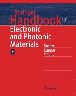
Springer Handbook of Electronic and Photonic Materials
Springer-Verlag New York Inc.
978-0-387-26059-4 (ISBN)
- Titel erscheint in neuer Auflage
- Artikel merken
Contributions from well known and respected researchers throughout the world
Thorough coverage of electronic and opto-electronic materials that today's electrical engineers, material scientists and physicists need
Interdisciplinary approach encompasses research in disciplines such as materials science, electrical engineering, chemical engineering, mechanical engineering, physics and chemistry
Safa Kasap is currently a Professor and Canada Research Chair in Electronic Materials and Devices in the Electrical Engineering Department at the University of Saskatchewan, Canada. He obtained his BSc (1976), MSc (1978) and PhD (1983) degrees from the Imperial College of Science, Technology and Medicine, University of London, specializing in amorphous semiconductors and chalcogenide glasses. In 1996 he was awarded the DSc (Engineering) from London University for his research contributions to materials science in electrical engineering. He is a Fellow of the Institution of Electrical Engineers, the Institute of Physics and the Institute of Materials. His research interests are in amorphous semiconductors, glasses for photonics, photoconductors, electrical, optical and thermal properties of materials, and related topics, with more than one hundred refereed journal papers in these areas. He is the Deputy Editor of the Journal of Materials Science: Materials in Electronics (Springer), and a Series Editor for the Series on Materials in Electronic and Optoelectronics (Wiley). Peter Capper has worked for the same company (through several name changes) for over 30 years in the area of II-VI compounds for infrared applications, latterly as a Materials Team Leader in charge of group of scientists working on the growth and characterisation of these compounds. This has been mainly in the area of cadmium mercury telluride and cadmium telluride, the premier infrared materials, by a range of bulk and epitaxial techniques. He has given several invited talks in Japan, USA and Europe, has coauthored over 100 Journal papers, holds one patent and has edited/written 5 books in the field since 1987. He is on the Editorial Board of the J. Mater. Sci.: Mater. Electron. (Springer) and is a Series Editor for Wiley on Materials for Electronics and Optoelectronics.
Each chapter has a concise summary that provides a general overview of the subject in the chapter in a clear language. The chapters begin at fundamentals and build up towards advanced concepts and applications. Emphasis is on physical concepts rather than extensive mathematical derivations. Each chapter is full of clear color illustrations that convey the concepts and make the subject matter enjoyable to read and understand. Examples in the chapters have practical applications. Chapters also have numerous extremely useful tables that summarize equations, experimental techniques, and most importantly, properties of various materials. The chapters have been divided into five parts. Each part has chapters that form a coherent treatment of a given area.
Chap. 1 Introduction: Perspectives on Electronic, Optoelectronic, and Photonic Materials
Part A: Fundamental Electronic, Optical, and Magnetic Properties
Part A contains chapters starting from basic concepts and build up to up-to-date knowledge in a logical easy to follow sequence. Part A would be equivalent to a graduate level treatise that starts from basic structural properties to go onto electrical, dielectric, optical, and magnetic properties. Each chapter starts by assuming someone who has completed a degree in physics, chemistry, engineering, or materials science.
Chap. 2 Electrical Conduction in Metals and Semiconductors.- Chap. 3 Optical Properties: Fundamentals and Characterization.- Chap. 4 Magnetic Properties.- Chap. 5 Defects in Monocrystalline Silicon.- Chap. 6 Diffusion in Semiconductors.- Chap. 7 Photoconductivity in Materials Research.- Chap. 8 Electronic Properties of Semiconductor Interfaces.- Chap. 9 Description of Charge Transport in Disordered Materials.- Chap. 10 Dielectric Response -- An Overview.- Chap. 11 Ionic Conduction and Applications
Part B: Growth and Characterization
Part B provides a clear overview of bulk and single-crystal growth, growth techniques (epitaxial crystal growth: LPE, MOVPE, MBE), and the structural, chemical, electrical and thermal characterization of materials. Silicon and II – VI compounds and semiconductors are especially emphasized.
Chap. 12 Bulk Crystal Growth.- Chap. 13 Single Crystal Silicon: Growth and Properties.- Chap. 14 Epitaxial Crystal Growth: LPE, MOVPE, MBE.- Chap. 15 II – VI Compounds: Growth.- Chap. 16 Wide Bandgap II – VI Semiconductors: Growth and Properties.- Chap. 17 Structural Characterization.- Chap. 18 Chemical Analysis.- Chap. 19 Thermal Properties and Characterization.- Chap. 20 Electrical Characterization of Semiconductor Materials and Devices
Part C: Materials for Electronics
Part C covers specific materials such as crystalline Si, microcrystalline Si, GaAs, high-temperature semiconductors, amorphous semiconductors, ferroelectric materials, and thin and thick films.
Chap. 21 Single Crystal Silicon.- Chap. 22 Silicon/Germanium.- Chap. 23 Gallium Arsenide.- Chap. 24 High Temperature Electronic Materials: Silicon Carbide and Diamond.- Chap. 25 Amorphous Semiconductors.- Chap. 26 Amorphous and Microcrystalline Silicon - Preparation and Properties for Devices.- Chap. 27 Ferroelectric Materials.- Chap. 28 Dielectric Materials for Microelectronics.- Chap. 29 Thin Films.- Chap. 30 Thick Films
Part D: Materials for Optoelectronics and Photonics
Part D examines materials that have applications in optoelectronics and photonics. It covers some of the state-of-the-art developments in optoelectronic materials, and covers III – V Ternaries, III-Nitrides, II – VI compounds, quantum wells, photonic crystals, glasses for photonics, nonlinear photonic glasses, nonlinear organic, and luminescent materials.
Chap. 31 III – V Ternary and Quaternary Compounds.- Chap. 32 Group III Nitrides.- Chap. 33 Electron Transport Within the III – V Nitride Semiconductors, GaN, AlN, and InN: A Monte Carlo Analysis.- Chap. 34 Cd-based wide bandgap compounds.- Chap. 35 Doping Aspects of Zn-Based Wide Bandgap Semiconductors.- Chap. 36 II – VI Narrow Bandgap Semiconductors: Optoelectronics.- Chap. 37 Optoelectronic Devices and Materials.- Chap. 38 Liquid Crystals.- Chap. 39 Organic Photoconductors.- Chap. 40 Luminescent Materials.- Chap. 41 Nanoengineered Tunable Photonic Crystals in the Near-IR and Visible.- Chap. 42 Quantum Wells, Superlattices and Bandgap Engineering.- Chap. 43 Glasses for Photonic Integration.- Chap. 44 Optical Nonlinearity in Photonic Glasses.- Chap. 45 Nonlinear Optoelectronic Materials
Part E: Novel Materials and Selected Applications
Part E provides a survey on novel materials and applications such as information recording devices (CD, video, DVD) as well as phase-change optical recording. The chapters also include applications such as solar cells, sensors, photoconductors, and carbon nanotubes. Both ends of the spectrum from research to applications are represented in chapters on molecular electronics and packaging materials.
Chap. 46 Solar Cells and Photovoltaics.- Chap. 47 Silicon on Mechanically Flexible Substrates for Large Area Electronics.- Chap. 48 Photoconductors for X-ray Image Detectors.- Chap. 49 Phase-change Optical Recording.- Chap. 50 Carbon Nanotubes and Bucky Materials.- Chap. 51 Magnetic Information Storage Materials.- Chap. 52 High-Temperature Superconductors.- Chap. 53 Molecular Electronics.- Chap. 54 Organic Materials for Chemical Sensing.- Chap. 55 Packaging Materials
Glossary of Terms
About the Authors
Subject Index
| Erscheint lt. Verlag | 19.10.2006 |
|---|---|
| Reihe/Serie | Springer Handbook of Electronic and Photonic Materials | 1.20 |
| Mitarbeit |
Anpassung von: C. Koughia |
| Zusatzinfo | 168 Tables, color; LXVIII, 1407 p. With CD-ROM. In 2 volumes, not available separately. |
| Verlagsort | New York, NY |
| Sprache | englisch |
| Maße | 203 x 276 mm |
| Themenwelt | Technik ► Elektrotechnik / Energietechnik |
| Technik ► Maschinenbau | |
| ISBN-10 | 0-387-26059-5 / 0387260595 |
| ISBN-13 | 978-0-387-26059-4 / 9780387260594 |
| Zustand | Neuware |
| Haben Sie eine Frage zum Produkt? |
aus dem Bereich


