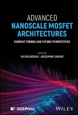
Advanced Nanoscale MOSFET Architectures
Wiley-IEEE Press (Verlag)
978-1-394-18894-9 (ISBN)
- Titel ist leider vergriffen;
keine Neuauflage - Artikel merken
Advanced Nanoscale MOSFET Architectures provides an in-depth review of modern metal–oxide–semiconductor field-effect transistor (MOSFET) device technologies and advancements, with information on their operation, various architectures, fabrication, materials, modeling and simulation methods, circuit applications, and other aspects related to nanoscale MOSFET technology.
The text begins with an introduction to the foundational technology before moving on to describe challenges associated with the scaling of nanoscale devices. Other topics covered include device physics and operation, strain engineering for highly scaled MOSFETs, tunnel FET, graphene based field effect transistors, and more. The text also compares silicon bulk and devices, nanosheet transistors and introduces low-power circuit design using advanced MOSFETs.
Additional topics covered include:
High-k gate dielectrics and metal gate electrodes for multi-gate MOSFETs, covering gate stack processing and metal gate modification
Strain engineering in 3D complementary metal-oxide semiconductors (CMOS) and its scaling impact, and strain engineering in silicon–germanium (SiGe) FinFET and its challenges and future perspectives
TCAD simulation of multi-gate MOSFET, covering model calibration and device performance for analog and RF applications
Description of the design of an analog amplifier circuit using digital CMOS technology of SCL for ultra-low power VLSI applications
Advanced Nanoscale MOSFET Architectures helps readers understand device physics and design of new structures and material compositions, making it an important resource for the researchers and professionals who are carrying out research in the field, along with students in related programs of study.
Kalyan Biswas, PhD, is an Assistant Professor in the ECE Department at MCKV Institute of Engineering in Liluah, Howrah, WB, India. Angsuman Sarkar, PhD, is a Professor in the ECE Department of the Kalyani Government Engineering College in Kalyani, Nadia, WB, India. He is a co-editor of the Wiley title Optical Switching: Device Technology and Applications in Networks (2022).
About the Editors xi
List of Contributors xiii
Preface xvii
Acknowledgments xix
1 Emerging MOSFET Technologies 1
Kalyan Biswas and Angsuman Sarkar
1.1 Introduction: Transistor Action 1
1.2 MOSFET Scaling 1
1.3 Challenges in Scaling the MOSFET 2
1.4 Emerging MOSFET Architectures 3
1.4.5 Graphene FET 7
1.4.6 III-V Material-based MOSFETS 7
1.4.7 HEMT 8
1.4.8 Strain Engineered MOSFETs 8
1.5 Organization of this Book 9
2 MOSFET: Device Physics and Operation 15
Ruthramurthy Balachandran, Savitesh M. Sharma, and Avtar Singh
2.1 Introduction to MOSFET 15
2.2 Advantages of MOSFET 16
2.3 Applications of MOSFETs 16
2.4 Types of MOSFETs 17
2.5 Band Diagram of MOSFET 19
2.6 MOSFET Regions of Operation 22
2.7 Scaling of MOSFET 25
2.8 Short-channel Effects 27
2.9 Body Bias Effect 31
2.10 Advancement of MOSFET Structures 33
3 High-K Dielectrics in Next Generation VLSI/Mixed Signal Circuits 47
Asutosh Srivastava
3.1 Introduction to Gate Dielectrics 47
3.2 High-K Dielectrics in Metal-Oxide-Semiconductor Capacitors 49
3.3 High-K Dielectrics in Metal Insulator Metal (MIM) Capacitors 50
3.4 MOSFETs Scaling and the Need of High-K 52
3.5 High-K Dielectrics in Next Generation Transistors 53
4 Consequential Effects of Trap Charges on Dielectric Defects for MU-G FET 61
Annada S. Lenka and Prasanna K. Sahu
4.1 Introduction 61
4.2 TID Effects Overview 63
4.3 Application Area of Device for TID Effect Analysis 64
4.4 Near the Earth: Trapped Radiation 66
4.5 Ionizing Radiation Effect in Silicon Dioxide (SiO2) 68
4.6 TID Effects in CMOS 70
4.7 TID Effects in Bipolar Devices 70
4.8 Understanding and Modeling a-SiO2 Physics 76
4.9 Hydrogen (H2) Reaction with Trapped Charges at Insulator 78
4.10 Pre-Existing Trap Density and their Respective Location 78
4.11 Use of High-K Dielectric in MU-G FET 79
4.12 Properties of Trap in the High-K with Interfacial Layer 80
4.13 Trap Extraction Techniques 81
4.14 Conclusion 81
5 Strain Engineering for Highly Scaled MOSFETs 85
Chinmay K. Maiti, Taraprasanna Dash, Jhansirani Jena, and Eleena Mohapatra
5.1 Introduction 85
5.2 Simulation Approach 88
5.3 Case Study 92
5.4 Conclusions 109
6 TCAD Analysis of Linearity Performance on Modified Ferroelectric Layer in FET Device with Spacer 113
Yash Pathak, Kajal Verma, Bansi Dhar Malhotra, and Rishu Chaujar
6.1 Introduction 113
6.2 Simulation and Structure of Device 114
6.3 Results and Analysis 115
6.4 Conclusion 120
7 Electrically Doped Nano Devices: A First Principle Paradigm 125
Debarati D. Roy, Pradipta Roy, and Debashis De
7.1 Introduction 125
7.2 Electrical Doping 128
7.3 First Principle 130
7.4 Molecular Simulation 136
7.5 Conclusion 137
8 Tunnel FET: Principles and Operations 143
Zahra Ahangari
8.1 Introduction to Quantum Mechanics and Principles of Tunneling 143
8.2 Tunnel Field-Effect Transistor 145
8.3 Challenges of Tunnel Field-Effect Transistor 148
8.4 Techniques for Improving Electrical Performance of Tunnel Field-Effect Transistor 151
8.5 Conclusion 169
9 GaN Devices for Optoelectronics Applications 175
Nagarajan Mohankumar and Girish S. Mishra
9.1 Introduction 175
9.2 Properties of GaN-Based Material 176
9.3 GaN LEDs 182
9.4 GaN Lasers 187
9.5 GaN HEMTs for Optoelectronics 189
9.6 GaN Sensors 191
10 First Principles Theoretical Design on Graphene-Based Field-Effect Transistors 201
Yoshitaka Fujimoto
10.1 Introduction 201
10.2 Graphene 202
10.3 Graphene/h-BN Hybrid Structure 206
10.4 Conclusions 217
11 Performance Analysis of Nanosheet Transistors for Analog ICs 221
Yogendra P. Pundir, Arvind Bisht, and Pankaj K. Pal
11.1 Introduction 221
11.2 Evolution of Nanosheet Transistors 222
11.3 TCAD Modeling of Nanosheet Transistor 230
11.4 Transistor’s Analog Performance Parameters 234
11.5 Challenges and Perspectives of Modern Analog Design 239
12 Low-Power Analog Amplifier Design using MOS Transistor in the Weak Inversion Mode 255
Soumya Pandit and Koyel Mukherjee
12.1 Introduction 255
12.2 Review of the Theory ofWeak Inversion Mode Operation of MOS Transistor 256
12.3 Design Steps for Transistor Sizing Using the IC 266
12.4 Design Examples 267
12.5 Summary 279
13 Ultra-conductive Junctionless Tunnel Field-effect Transistor-based Biosensor with Negative Capacitance 281
Palasri Dhar, Soumik Poddar, and Sunipa Roy
13.1 Introduction 281
13.2 Importance of SS and ION/IOFF in Biosensing 284
13.3 Importance of Dopingless Source and Drain in High Conductivity 287
13.4 Relation of Negative Capacitance with Non-hysteresis and Effect on Biosensing 289
13.5 Variation of Source Material on Biosensing 290
13.6 Importance of Dual Gate and Ferroelectricity on Biosensing 291
13.7 Effect of Dual Material Gate on Biosensing 296
14 Conclusion and Future Perspectives 301
Kalyan Biswas and Angsuman Sarkar
14.1 Applications 301
14.2 Some Recent Developments 303
14.3 Future Perspectives 306
14.4 Conclusion 307
References 308
Index 311
| Erscheinungsdatum | 29.05.2024 |
|---|---|
| Sprache | englisch |
| Gewicht | 737 g |
| Themenwelt | Technik ► Elektrotechnik / Energietechnik |
| Technik ► Maschinenbau | |
| ISBN-10 | 1-394-18894-3 / 1394188943 |
| ISBN-13 | 978-1-394-18894-9 / 9781394188949 |
| Zustand | Neuware |
| Haben Sie eine Frage zum Produkt? |
aus dem Bereich


