Ultra Clean Processing of Semiconductor Surfaces XVI
Trans Tech Publications Ltd (Verlag)
978-3-0364-0312-0 (ISBN)
- Titel nicht im Sortiment
- Artikel merken
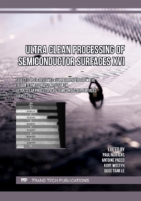
Selected peer-reviewed full text papers from the 16th International Symposium on Ultra Clean Processing of Semiconductor Surfaces (UCPSS 2023), September 12-14, 2023, Brugge, Belgium
This proceedings volume contains the proceedings of all presentations of the 16th International Symposium on Ultra Clean Processing of Semiconductor Surfaces (UCPSS) 2023. The subject matter of the UCPSS symposium is ultra-clean processing, isotropic selective etching and surface preparation technology in all steps of the fabrication of micro-and nano-electronic integrated circuits.This volume describes the recent progress in the field of ultra clean surfaces, surface cleaning and preparation for the production of micro- and nano-electronic integrated circuits and related subjects. This involves a wide variety of surfaces of mixed composition and with nano-topography. The goal of the processes is to obtain nano precise etching and cleaning resulting in ultra clean surfaces with a very high degree of perfection, i.e. with minimal amounts of residues or defects. This comprises different surface and cleaning steps throughout the entire device manufacturing process.
Preface
Chapter 1: Progress in Semiconductor Technologies
Past, Present, and Future of Semiconductor Cleaning Technology
Nanosheet-Based Transistor Architectures for Advanced CMOS Scaling: Wet Etch and Gas Phase Etch Challenges in Confined Spaces
On Gas-Phase Selective Dry Etching in 3D Inflections
Chapter 2: Selective Etching of SiGe Alloy Semiconductors
SiGe Selective Etching to Enable Bottom and Middle Dielectric Isolations for Advanced Gate-All-Around FET Architecture
Selectivity Tuning by Peroxide Concentration for the Selective Etching of SiGe20 to Si and SiGe40 to SiGe20
Investigation of Selective Wet Etching of SiGe Substrates for High-Performance Device Manufacturing
Highly Selective Etching of SiGe to Si for GAAFET
Chapter 3: Surface Chemistry of Group IV Semiconductors
Atomic Level Chemical and Structural Properties of Silicon Surface and Initial Stages of Oxidation
Effects of Ultrahigh Vacuum Treatments on Wet Chemically Cleaned Si Surfaces
Silicon and Germanium Corrosion by Fluorinated Chemistry in Presence of Wafer Charging
Study on Alternative Dipole Material Wet Clean by pH Controlled Functional Water
Reaction Mechanism Analysis of Si Selective Etching for Gate-All-Around Transistors by Molecular Simulations
Chapter 4: Surface Chemistry of Compound Semiconductors
Surface Characterization - Gallium Nitride Depth Profiling with LEIS
Effect of Post-Etch Wet Cleaning on GaAs Surfaces
Chapter 5: Pattern Collapse in Semiconductor Device Manufacturing
Pattern Collapse Simulation in CMOS Image Sensors Devices
Observation of Capillary Condensation and Pattern Bending Phenomena in Si Nanopillars Using In Situ TEM
Improvement of Fingering-Induced Pattern Collapse by Adjusting Chemical Mixing Procedure
Modeling of Capillary Pattern Collapse on Sub-5nm Pillars Using Molecular Dynamics
Insights into FinFET Structure Collapse: A Reactive Force Field-Based Molecular Dynamics Investigation
Chapter 6: Etching of Dielectrics
Silicon Nitride Selective Functionalization with Aqueous Cellulose
Selective Si3N4 Etching for 3D NAND Integration by Using Low Concentration of H3PO4
Investigation of Oxide Regrowth in the Selective Si3N4 Etching Process for 3D NAND Fabrication by Using Finite Element Modeling Simulation
Methods for Uniform Wet Etching in Narrow Trenches and Vias
Chapter 7: Assessment and Control of Contaminations in Technological Fluids and Air
Application of Hydrosol to Aerosol Based Metrology to Predict Wafer Defects from Process Chemical Contamination
Nanoparticle Analyzing Technique Review and Sub-10 nm Nanoparticle Sizing Methods Comparison
On-Line Metal Concentration Measurement at an Ultra-Trace Level in DIW by Solid Phase Extraction Method Coupled with ICP-MS
Real Time AMC Monitoring with Novel Chemical Ionization Mass Spectrometry at Single-Digit pptv Concentrations
Monitoring of Trace Molecular Impurities in Clean-Room Air
Investigation of Effects of Sulfuric Acid in Single Wafer Cleaning Process Using Isopropyl Alcohol
Chapter 8: Contaminations on Wafer Surfaces
Direct Analysis of Si, SiC and GaN Wafers by LA-GED-MSAG-ICP-MS
Chemical Identification of Sub-20 nm Defects and Sub-Monolayer Residues with Nano IR PiFM
Development of Intentional Contamination in Iron by Bath for Silicon Wafers and Evaluation of VPD-Bulk and LPD-Bulk for Metallic Contaminants Analyses by ICPMS
Defect Mapping and Densification in Self-Assembled Monolayers of Octadecyltrichlorosilane on SiO2
Fine Edge and Bevel Film Cut Accuracy by a Novel and High Precision Wafer Centering System
Chapter 9: Modelling of Wet Etching and Cleaning Processes
Fluid Simulation over a Rotating Disk: Momentum and Mass Transfer across the Wafer Boundary
Etch Profile Prediction Model Using Convolutional Neural Network
ESD Prevention Technology for Two-Fluid Pure Water Spray Cleaning with Controlled Electrostatic Charge
Chapter 10: Particle Removal
Parametric Studies on Particle Removal and Erosion in Nozzle Injection Megasonic Cleaning
Optimal Injection Distance in Ultrasonic Water Flow Cleaning
Design of “Soft” Cleaning Processes for Emerging Substrates via Stimuli Responsive Chemistry
Evaluation and Optimization of Particle Removal with a Resist Peeling Method
Pinpoint Particle Removal for EUV Pellicle Productivity Enhancement
Electrostatic-Induced Particle Behavior Simulation Framework in Cleaning Process: Interaction between Solid-Liquid Interfaces
Chapter 11: Sustainability Aspects in Wet Processing
Sulfuric Acid Reduction in Post-Ash Cleans
Reduction of Process Chemicals and Energy Use in Single-Wafer Process Applications
Eco-Friendly SPM Alternative Resist Stripping with High-Concentration O3-Water Technology
Chapter 12: Materials and Technologies for Interconnects
Slurry Activation for Enhanced Surface Redox Reactions in CMP
New Quaternary Amines and Solvents for Photoresist Developing and Stripping Applications
Alkali Wet Chemicals for Ru with Advanced Semiconductor Technology Nodes
Wet Cleaning of Ru Semi-Damascene 18 MP Structures
A Cleaning Method for Post-Etch Ruthenium Residue Removal Using UV and Liquid Chemical
Wet Cleaning/Etching of NiAl Thin Film
Plasma Oxidation of Patterned Mo Nanowires for Precise and Uniform Dry Etching
Controlled and Uniform Wet Etching of Molybdenum Nanowires
Selective Removal of Various Resilient Ionic and Halides-Based Surface Contaminants by Wet Cleaning
| Erscheinungsdatum | 15.09.2023 |
|---|---|
| Reihe/Serie | Solid State Phenomena |
| Zusatzinfo | Illustrations, unspecified |
| Verlagsort | Zurich |
| Sprache | englisch |
| Maße | 170 x 240 mm |
| Gewicht | 790 g |
| Themenwelt | Technik ► Elektrotechnik / Energietechnik |
| Technik ► Maschinenbau | |
| ISBN-10 | 3-0364-0312-4 / 3036403124 |
| ISBN-13 | 978-3-0364-0312-0 / 9783036403120 |
| Zustand | Neuware |
| Haben Sie eine Frage zum Produkt? |
aus dem Bereich


