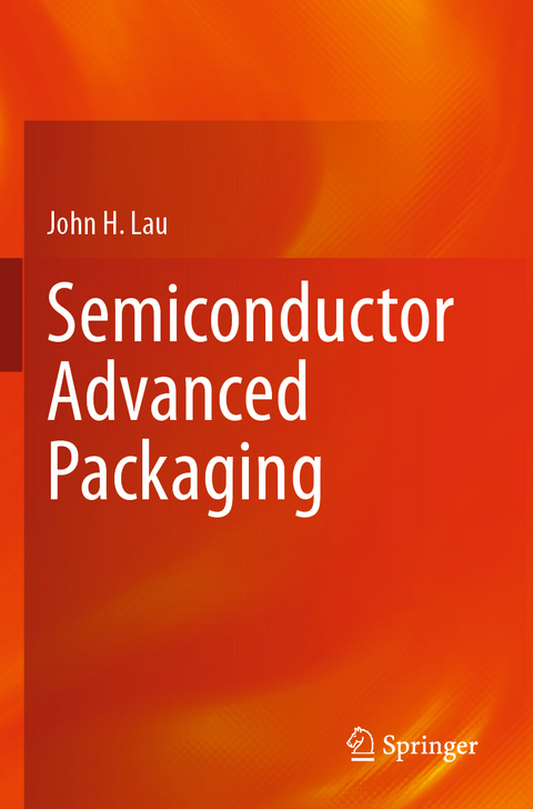
Semiconductor Advanced Packaging
Springer Verlag, Singapore
978-981-16-1378-4 (ISBN)
John H. Lau, Ph.D., P.E. has been the CTO of Unimicron in Taiwan since August 2019. Prior to that, he was a Senior Technical Advisor at ASM Pacific Technology in Hong Kong for 5 years; a specialist of the Industrial Technology Research Institute in Taiwan for 4½ years and a Senior Scientist/MTS at Hewlett-Packard Laboratory/Agilent in California for more than 25 years. He earrned a Ph.D. degree in theoretical and applied mechanics from the University of Illinois at Urbana–Champaign.With more than 40 years of R&D and manufacturing experience, he has authored or coauthored more than 480 peer-reviewed technical publications, invented more than 30 issued or pending US patents, and given more than 300 lectures/workshops/keynotes worldwide. He has authored or coauthored 20 textbooks on fan-out wafer-level packaging, 3D IC heterogeneous integration and packaging, TSV for 3D integration, advanced MEMS packaging, reliability of 2D and 3D IC interconnects, flip chip, WLP, MCM, area-array packages, WLCSP, high-density PCB, SMT, DCA, TAB, lead-free materials, soldering, manufacturing, and solder joint reliability. He has received many awards from the American Society of Mechanical Engineers (ASME), the Institute of Electrical and Electronics Engineers (IEEE), the Society of Manufacturing Engineers (SME) and other societies. He is an elected ASME fellow, IEEE fellow, and IMAPS fellow, and has been heavily involved in many of ASME’s, IEEE’s, and IMAPS’ technical activities.
Recent Advance on Semiconductor Packaging.- System-in-Package.- Fan-In Wafer/Panel-Level Chip-Scale Packages.- Fan-Out Wafer/Panel-Level Packaging.- 2D, 2.1D, and 2.3D IC Integration.- 2.5D IC Integration.- 3D IC Integration.- Hybrid Bonding.- Chiplets Packaging.- Dielectric Materials.- Trends and Roadmap for Advanced Semiconductor Packaging.
| Erscheinungsdatum | 23.05.2022 |
|---|---|
| Zusatzinfo | 530 Illustrations, color; 27 Illustrations, black and white; XXII, 498 p. 557 illus., 530 illus. in color. |
| Verlagsort | Singapore |
| Sprache | englisch |
| Maße | 155 x 235 mm |
| Themenwelt | Technik ► Elektrotechnik / Energietechnik |
| Technik ► Maschinenbau | |
| Schlagworte | 2D, 2.1D, 2.3D, 2.5D, and 3D IC Integration • Fan-in Wafer/Panel-Level Chip-Scale Package • Fan-out Wafer/Panel-Level Packaging • Flip Chip Technology • Heterogenenous Chiplets Integration • High Bandwidth Memeory • System-in-Package • Thermocompression Bonding and Chip-to-Wafer Bonding • Through-silicon Vias and Redistribution-Layers • Wafer-to-Wafer Bondind and Hybrid Bonding |
| ISBN-10 | 981-16-1378-8 / 9811613788 |
| ISBN-13 | 978-981-16-1378-4 / 9789811613784 |
| Zustand | Neuware |
| Haben Sie eine Frage zum Produkt? |
aus dem Bereich


