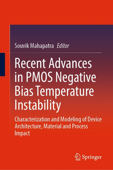
Recent Advances in PMOS Negative Bias Temperature Instability (eBook)
XXIII, 311 Seiten
Springer Singapore (Verlag)
978-981-16-6120-4 (ISBN)
This book covers advances in Negative Bias Temperature Instability (NBTI) and will prove useful to researchers and professionals in the semiconductor devices areas. NBTI continues to remain as an important reliability issue for CMOS transistors and circuits. Development of NBTI resilient technology relies on utilizing suitable stress conditions, artifact free measurements and accurate physics-based models for the reliable determination of degradation at end-of-life, as well as understanding the process, material and device architectural impacts. This book discusses:
- BTI Analysis Tool (BAT), a comprehensive physics-based framework, to model the measured time kinetics of parametric drift during and after DC and AC stress, at different stress and recovery biases and temperature, as well as pulse duty cycle and frequency.
- The Reaction Diffusion (RD) model is used for generated interface traps, Transient Trap Occupancy Model (TTOM) for charge occupancy of the generated interface traps and their contribution, Activated Barrier Double Well Thermionic (ABDWT) model for hole trapping in pre-existing bulk gate insulator traps, and Reaction Diffusion Drift (RDD) model for bulk trap generation in the BAT framework; NBTI parametric drift is due to uncorrelated contributions from the trap generation (interface, bulk) and trapping processes.
Souvik Mahapatra received his Bachelors and Masters degrees in Physics from Jadavpur University, Calcutta, India in 1993 and 1995 respectively, and PhD in Electrical Engineering from IIT Bombay, Mumbai, India in 1999. During 2000-2001, he was with Bell Laboratories, Lucent Technolgies, Murray Hill, NJ, USA. Since 2002 he is with IIT Bombay, and is currently the PK Kelkar Chair Professor in the Department of Electrical Engineering. His primary research interests are in the areas of semiconductor device characterization, modeling and simulation, and in particular, MOS transistor and Flash memory device scaling and reliability. He has interacted closely with major semiconductor industries in the world, and has contributed in several technologically relevant research topics such as MOS gate insulator scaling, Bias Temperature Instability and Hot Carrier Degradation in CMOS devices, CHISEL NOR Flash, SONOS NOR and NAND Flash memory devices. He has authored and co-authored more than 190 papers in peer reviewed journals and conferences and several book chapters, and delivered invited talks and tutorials in major international conferences around the world, including at the IEEE IEDM and IEEE IRPS. He has served as a distinguished lecturer of the IEEE EDS, chair of the IEEE EDS device reliability physics subcommittee, and in paper selection subcommittees and as session chairs in several IEEE conferences. He is a fellow of Institute of Electrical and Electronics Engineers (IEEE), Indian National Science Academy (INSA), Indian National Academy of Engineering (INAE) and Indian Academy of Sciences (IASc).
This book covers advances in Negative Bias Temperature Instability (NBTI) and will prove useful to researchers and professionals in the semiconductor devices areas. NBTI continues to remain as an important reliability issue for CMOS transistors and circuits. Development of NBTI resilient technology relies on utilizing suitable stress conditions, artifact free measurements and accurate physics-based models for the reliable determination of degradation at end-of-life, as well as understanding the process, material and device architectural impacts. This book discusses: Ultra-fast measurements and modelling of parametric drift due to NBTI in different transistor architectures: planar bulk and FDSOI p-MOSFETs, p-FinFETs and GAA-SNS p-FETs, with Silicon and Silicon Germanium channels. BTI Analysis Tool (BAT), a comprehensive physics-based framework, to model the measured time kinetics of parametric drift during and after DC and ACstress, at different stress and recovery biases and temperature, as well as pulse duty cycle and frequency. The Reaction Diffusion (RD) model is used for generated interface traps, Transient Trap Occupancy Model (TTOM) for charge occupancy of the generated interface traps and their contribution, Activated Barrier Double Well Thermionic (ABDWT) model for hole trapping in pre-existing bulk gate insulator traps, and Reaction Diffusion Drift (RDD) model for bulk trap generation in the BAT framework; NBTI parametric drift is due to uncorrelated contributions from the trap generation (interface, bulk) and trapping processes. Analysis and modelling of Nitrogen incorporation into the gate insulator, Germanium incorporation into the channel, and mechanical stress effects due to changes in the transistor layout or device dimensions; similarities and differences of (100) surface dominated planar and GAA MOSFETs and (110) sidewall dominated FinFETs are analysed.
| Erscheint lt. Verlag | 25.11.2021 |
|---|---|
| Zusatzinfo | XXIII, 311 p. 213 illus., 189 illus. in color. |
| Sprache | englisch |
| Themenwelt | Naturwissenschaften ► Chemie ► Analytische Chemie |
| Naturwissenschaften ► Physik / Astronomie | |
| Technik ► Elektrotechnik / Energietechnik | |
| Schlagworte | ABDWT model • Charge Pumping • DCIV • Dimension Scaling • FDSOI • FinFET • flicker noise • GAA-SNS FET • HKMG • Layout • Mechanical strain • MOSFET • NBTI • RDD model • RD model • Si channel • SiGe channel • SILC • Trap Generation • Trapping |
| ISBN-10 | 981-16-6120-0 / 9811661200 |
| ISBN-13 | 978-981-16-6120-4 / 9789811661204 |
| Informationen gemäß Produktsicherheitsverordnung (GPSR) | |
| Haben Sie eine Frage zum Produkt? |
Größe: 17,6 MB
DRM: Digitales Wasserzeichen
Dieses eBook enthält ein digitales Wasserzeichen und ist damit für Sie personalisiert. Bei einer missbräuchlichen Weitergabe des eBooks an Dritte ist eine Rückverfolgung an die Quelle möglich.
Dateiformat: PDF (Portable Document Format)
Mit einem festen Seitenlayout eignet sich die PDF besonders für Fachbücher mit Spalten, Tabellen und Abbildungen. Eine PDF kann auf fast allen Geräten angezeigt werden, ist aber für kleine Displays (Smartphone, eReader) nur eingeschränkt geeignet.
Systemvoraussetzungen:
PC/Mac: Mit einem PC oder Mac können Sie dieses eBook lesen. Sie benötigen dafür einen PDF-Viewer - z.B. den Adobe Reader oder Adobe Digital Editions.
eReader: Dieses eBook kann mit (fast) allen eBook-Readern gelesen werden. Mit dem amazon-Kindle ist es aber nicht kompatibel.
Smartphone/Tablet: Egal ob Apple oder Android, dieses eBook können Sie lesen. Sie benötigen dafür einen PDF-Viewer - z.B. die kostenlose Adobe Digital Editions-App.
Buying eBooks from abroad
For tax law reasons we can sell eBooks just within Germany and Switzerland. Regrettably we cannot fulfill eBook-orders from other countries.
aus dem Bereich


