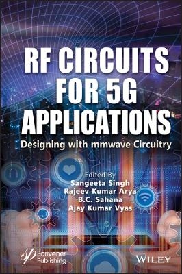
RF Circuits for 5G Applications
Wiley-Scrivener (Verlag)
978-1-119-79192-8 (ISBN)
- Titel ist leider vergriffen;
keine Neuauflage - Artikel merken
The wireless communication sector is experiencing exponential expansion, particularly in the areas of mobile data and the 5G mobile network, creating fresh market possibilities for designing the integrated circuits (ICs) needed in the industry. Drawing from scientific literature and practical realization, this book explores FinFET-based analog IC designing for 5G communication networks and considers the latest breakthroughs and obstacles. It also presents the recent research trends and future roadmaps for the 5G communication circuits.
RF Circuits for 5G Applications includes design guidelines to be considered when designing these circuits and detrimental scaling effects of the same. In addition, to enhance the usability of this book, the editors have included real-time problems in RFIC designing and case studies from experimental results, as well as clearly demarcated design guidelines for the 5G communication ICs designing.
Audience
The primary target audience includes researchers, postgraduate students, and industry professionals pursuing specializations in RF engineering, electronics engineering, electrical engineering, information, and communication technology.
Sangeeta Singh, PhD, is an assistant professor in the Department of Electronics and Communication Engineering, NIT Patna, India. She has been recognized as an eminent scholar in the field of electronics and computer engineering. She has published many research papers in reputed international journals and conferences, and has edited “CMOS Analog IC Design for 5G and Beyond” (2021). Rajeev Kumar Arya, PhD, received his doctorate in Communication Engineering from the Indian Institute of Technology (IIT Roorkee) in 2016. He is an assistant professor in the Department of Electronics & Communication Engineering at the National Institute of Technology, Patna, India. He has published many articles in international journals and conferences and received the Best Paper award at ICCET-2019. B.C. Sahana, PhD, is an assistant professor in the Department of Electronics and Communication Engineering, NIT Patna, India. He has supervised PhD, M.Tech, and B.Tech students in the area of signal processing, optimization, soft computing, and swarm intelligence techniques with applications to various engineering design problems, image processing and compression, computer vision, geophysical signal processing, and filter design. He has published more than 20 research publications in journals and conferences. Ajay Kumar Vyas, PhD, has more than 16 years of teaching and research experience. He is currently a senior assistant professor at the Adani Institute of Infrastructure Engineering, Ahmedabad, India. He has published several books on digital electronics and research papers in peer-reviewed international journals and conferences, and has edited five books.
Preface xv
Part I: 5G Communication 1
1 Needs and Challenges of the 5 th Generation Communication Network 3
Anamika Raj, Gaurav Kumar and Sangeeta Singh
1.1 Introduction 3
1.1.1 What is 5G and Do We Need 5G? 5
1.1.2 A Brief History of Gs 6
1.2 mmWave Spectrum, Challenges, and Opportunities 8
1.3 Framework Level Requirements for mmWave Wireless Links 11
1.4 Circuit Aspects 12
1.5 Outline of the Book 14
Acknowledgement 15
References 15
2 5G Circuits from Requirements to System Models and Analysis 19
Vipin Sharma, Rachit Patel and Krishna Pandey
2.1 RF Requirements Governed by 5G System Targets 19
2.2 Radio Spectrum and Standardization 20
2.3 System Scalability 21
2.4 Communication System Model for RF System Analysis 22
2.5 System-Level RF Performance Model 23
2.5.1 Transmitter, Receiver, Antenna Array and Transceiver Architectures for RF and Hybrid Beamforming 24
2.6 Radio Propagation and Link Budget 24
2.6.1 Radio Propagation Model 24
2.6.2 Link Budgeting 25
2.7 Multiuser Multibeam Analysis 26
2.8 Conclusion 28
Acknowledgement 29
References 29
3 Millimetre-Wave Beam-Space MIMO System for 5G Applications 31
G. Indumathi, J. Roscia Jeya Shiney and Shashi Kant Dargar
3.1 Introduction 32
3.2 Beam-Space Massive MIMO System 34
3.2.1 System Model 36
3.2.2 Saleh-Valenzuela Channel Model 37
3.3 Array Response Vector 37
3.3.1 mmWave Beam-Space Massive (mWBSM)-MIMO System 38
3.4 Discrete Lens Antenna Array 39
3.5 Beam Selection Algorithm 42
3.6 Mean Sum Assignment-Based Beam User Association 45
3.6.1 Performance Evaluation 46
3.7 Conclusion 49
References 49
Part II: Oscillator & Amplifier 53
4 Gain-Bandwidth Enhancement Techniques for mmWave Fully-Integrated Amplifiers 55
Shalu C., Shakti Sindhu and Amitesh Kumar
4.1 RLC Tank 56
4.1.1 RC Low-Pass (LP) Filter 56
4.1.2 RLC Band-Pass (BP) Filter 56
4.2 Coupled Resonators 57
4.2.1 Bode-Fano (B-F) Limit 57
4.2.2 Capacitively Coupled Resonators 59
4.2.3 Inductively Coupled Resonators 60
4.2.4 Magnetically Coupled Resonators 60
4.2.5 Magnetically and Capacitive Coupled Resonator 61
4.2.6 Coupled Resonators Comparison 62
4.3 Resonators Based on the Transformers 63
4.3.1 On the Parasitic Interwinding Capacitance 63
4.3.2 Effect of Unbalanced Capacitive Terminations 64
4.3.3 Frequency Response Equalization 65
4.3.4 On the Parasitic Magnetic Coupling in Multistage Amplifiers 66
4.3.5 Extension to Impedance Transformation 67
4.3.6 On the kQ Product 67
4.3.7 Transformer-Based Power Dividers (PDs) 68
4.3.8 Transformer-Based Power Combiners (PCs) 69
4.4 Conclusion 69
Acknowledgments 70
References 70
5 Low-Noise Amplifiers 73
Jyoti Priya, Sangeeta Singh and Bambam Kumar
5.1 Introduction 73
5.2 Basics of RFIC 75
5.2.1 Voltage Gain in dB 75
5.2.2 Power Gain in dB 75
5.2.3 Issues in RF Design 75
5.3 Structure of MOSFET 81
5.4 Bandwidth Estimation Techniques 84
5.5 Noise 88
5.5.1 Noise in MOSFET 89
5.6 Different Topologies of LNA 92
Conclusion 103
Acknowledgement 103
References 104
6 Mixer Design 107
Brajendra Singh Sengar and Amitesh Kumar
6.1 Introduction 107
6.2 Properties 109
6.3 Diode Mixer 114
6.4 Transistor Mixer 116
6.5 Conclusion 119
Acknowledgement 119
References 119
7 RF LC VCOs Designing 123
M. Sankush Krishna, Madhuraj Kumar, Neelesh Pratap Singh and Anjan Kumar
7.1 Introduction 124
7.1.1 Basic VCO Models 124
7.1.2 Phase Noise 125
7.1.3 Flicker Noise 126
7.1.4 Distributed Oscillators 128
7.2 Tuning Extension Techniques 129
7.2.1 Varactor 129
7.2.2 Switched Capacitors 130
7.2.3 Switched Inductors 131
7.2.4 Switched TLs 132
7.2.5 4th Order Tanks and Other Techniques 132
7.3 Conclusion 133
Acknowledgement 133
References 134
8 RF Power Amplifiers 137
Anchal Tyagi, Rachit Patel and Krishna Pandey
8.1 Specification 137
8.1.1 Efficiency 138
8.1.2 Generic Amplifier Classes 138
8.1.3 Heating 139
8.1.4 Linearity 139
8.1.5 Ruggedness 140
8.2 Bipolar PA Design 140
8.3 CMOS Power Amplifier Design 142
8.3.1 Performance Parameters 143
8.3.1.1 Linearity 143
8.3.1.2 Gain 143
8.3.1.3 Efficiency 144
8.3.1.4 Output Power 144
8.3.1.5 Power Consumption 144
8.3.2 Drawbacks of CMOS Power Amplifier 144
8.3.3 Design of CMOS Power Amplifier 145
8.3.3.1 Common Cascode PA Design 145
8.3.3.2 Self-Bias Cascode PA Design 146
8.3.3.3 Differential Cascode PA Design 147
8.3.3.4 Power Combining PA Design 147
8.4 Linearization Principles: Predistortion Technique, Phase-Correcting Feedback, Envelope Elimination and Restoration (EER), Cartesian Feedback 148
8.4.1 Predistortion Linearization Technique 148
8.4.2 Phase Correcting Feedback Technique 150
8.4.3 Cartesian Feedback Technique 151
8.4.4 Envelope Elimination and Restoration Technique 152
Acknowledgement 154
References 154
9 RF Oscillators 157
Pramila Jakhar and Amitesh Kumar
9.1 Introduction 157
9.2 Specifications 159
9.2.1 Frequency and Tuning 159
9.2.2 Tuning Constant and Linearity 159
9.2.3 Power Dissipation 160
9.2.4 Phase to Noise Ratio 160
9.2.5 Reciprocal Mixing 160
9.2.6 Signal to Noise Degradation of FM Signals Spurious Emission 161
9.2.7 Harmonics, I/Q Matching, Technology and Chip Area 161
9.3 LC Oscillators 162
9.3.1 Frequency, Tuning and Phase Noise Frequency Tuning Phase Noise to Carrier Ratio 163
9.3.2 Topologies 164
9.3.3 NMOS Only Cross-Coupled Structure 164
9.3.4 RC Oscillators 165
9.4 Design Examples 167
9.4.1 830 MHz Monolithic LC Oscillator Circuit Design Measurements 167
9.4.2 A 10 GHz I/Q RC Oscillator with Active Inductors 167
9.5 Conclusion 168
Acknowledgement 168
References 169
Part III: RF Circuit Applications 171
10 mmWave Highly-Linear Broadband Power Amplifiers 173
Shalu C., Shakti Sindhu and Amitesh Kumar
10.1 Basics of PAs 173
10.1.1 Single Transistor Amplifier 173
10.1.2 Trade-Offs Among Power Amplifier Design Parameters (P 0 , PAE and Linearity) 174
10.1.3 Harmonic Terminations and Switching Amplifiers 175
10.1.4 Challenges at Millimeter-Wave 177
10.2 Millimeter Wave-Based AB Class PA 177
10.2.1 Efficiency at Power Back-Off 178
10.2.2 Sources of AM-PM Distortion 178
10.2.3 Distortion Cancellation Techniques 179
10.2.3.1 Input PMOS Varactors 179
10.2.3.2 Complementary N-PMOS Amplifier 180
10.2.3.3 Degeneration Inductance 180
10.2.3.4 Harmonic Traps 180
10.3 Design Example: A Highly Linear Wideband PA in 28 nm CMOS 181
10.3.1 Transformer-Based Output Combiner and Inter-Stage Power Divider 182
10.3.2 More on the kQ Product 183
10.4 Conclusion 185
Acknowledgments 185
References 186
11 FinFET Process Technology for RF and Millimeter Wave Applications 189
A. Theja, Vikas A., Meena Panchore and Kanchan Cecil
11.1 Evaluation of FinFET Technology 189
11.1.1 Steps of Fabrication and Process Flow of FinFET Technology 191
11.1.2 Digital Performance 193
11.1.3 Analog/RF Performance 195
11.2 Distinct Properties of FinFET 197
11.2.1 Performance with Transistor Scaling 198
11.2.2 Nonlinear Gate Resistance by Three Dimensional Structure 199
11.2.3 Self-Heating Effect in FinFETs 202
11.3 Assessment of FinFET Technology for RF/mmWave Applications 203
11.3.1 RF Performance 204
13.3.1.1 Parasitic Extraction 206
11.3.2 Noise Performance 208
11.3.3 Noise Matching with Gain at the mmWave Frequency 210
11.4 Design Process of FinFET for RF/mmWave Performance Optimization 211
11.4.1 Cascaded Chain Design Consideration for Wireless System 212
11.4.2 Optimization of Noise Figure with G max for LNA Within Self-Heat Limit 213
11.4.3 Gain Per Power Efficiency 215
11.4.4 Linearity for Gain and Power Efficiency 217
11.4.5 Neutralization for mmWave Applications 219
References 220
12 Pre-Distortion: An Effective Solution for Power Amplifier Linearization 223
Gaurav Bhargava and Shubhankar Majumdar
12.1 Introduction 223
12.2 Standard Measures of Nonlinearity of Power Amplifier 224
12.2.1 Gain Compression Point (1 dB) 225
12.2.2 Harmonic and Intermodulation Distortion (IMD) 225
12.2.3 Third-Order Intercept Point (TOI) 227
12.2.4 AM/AM and AM/PM Distortion 227
12.2.5 Adjacent Channel Power Ratio (ACPR) 228
12.2.6 Error Vector Magnitude (EVM) 229
12.3 What is Linearization? 230
12.3.1 Feed Forward Linearization 230
12.3.2 Feedback Linearization 231
12.3.3 Pre-Distortion Linearization 231
12.4 Example of Analog Pre-Distortion-Based Class EFJ Power Amplifier 234
Conclusion and Future Scope 237
References 238
13 Design of Control Circuit for Mitigation of Shadow Effect in Solar Photovoltaic System 241
Dhvanit Bhavsar, Shubham Bhatt, Siddhi Vinayak Pandey and Alok Kumar Singh
13.1 Introduction 242
13.2 Proposed Methodology 246
13.3 Results and Discussion 260
13.4 Conclusion 263
Acknowledgement 263
References 264
Part IV: RF Circuit Modeling 267
14 HBT High-Frequency Modeling and Integrated Parameter Extraction 269
Ashish Bhatnagar and Rachit Patel
14.1 HBT High-Frequency Modeling and Integrated Parameter Extraction 269
14.2 High-Frequency HBT Modeling 270
14.2.1 DC and Small Signal Models 271
14.2.2 Linearized T-Model 272
14.2.3 Linearized Hybrid π model 272
14.3 Integrated Parameters Extraction 275
14.3.1 Formulation of Integrated Parameter Extraction 275
14.3.2 Optimization of Model 276
14.4 Noise Model Validation 276
14.5 Parameters Extraction of an HBT Model 276
Acknowledgement 277
References 277
15 Non-Linear Microwave Circuit Design Using Multi-Harmonic Load-Pull Simulation Technique 279
Veral Agarwal and Rachit Patel
15.1 Introduction 279
15.2 Multi-Harmonic Load-Pull Simulation Using Harmonic Balance 280
15.2.1 Formulation of Multi-Harmonic Load-Pull Simulation 280
15.2.2 Systematic Design Procedure 281
15.3 Application of Multiharmonic Load-Pull Simulation 282
15.3.1 Narrowband Power Amplifier Design 282
15.3.2 Frequency Doubler Design 285
References 287
16 Microwave RF Designing Concepts and Technology 289
Madhu Raj Kumar and Neelesh Pratap Singh
16.1 Introduction 289
16.1.1 Gain 290
16.1.2 Noise 290
16.1.3 Non Linearity 291
16.1.4 Sensitivity 295
16.2 Microwave RF Device Technology and Characterization 296
16.2.1 Characterization and Modeling 296
16.2.2 Modeling 296
16.2.3 Cut-Off Frequency 298
16.2.4 Maximum Oscillation Frequency 299
16.2.5 Input Limited Frequency 301
16.2.6 Output Limited Frequency 301
16.2.7 Maximum Available Frequency 302
16.2.8 Technology Choices 302
16.2.9 Double Poly Devices 303
16.3 Passive Components 303
16.3.1 Resistors 304
16.3.2 Capacitors 304
16.3.3 Inductors 307
Conclusion 309
Acknowledgement 309
References 309
Index 313
| Erscheinungsdatum | 12.04.2023 |
|---|---|
| Sprache | englisch |
| Gewicht | 730 g |
| Themenwelt | Technik ► Elektrotechnik / Energietechnik |
| ISBN-10 | 1-119-79192-8 / 1119791928 |
| ISBN-13 | 978-1-119-79192-8 / 9781119791928 |
| Zustand | Neuware |
| Haben Sie eine Frage zum Produkt? |
aus dem Bereich


