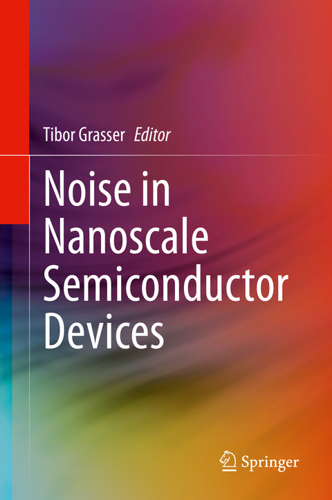
Noise in Nanoscale Semiconductor Devices (eBook)
VI, 724 Seiten
Springer-Verlag
978-3-030-37500-3 (ISBN)
This book summarizes the state-of-the-art, regarding noise in nanometer semiconductor devices. Readers will benefit from this leading-edge research, aimed at increasing reliability based on physical microscopic models. Authors discuss the most recent developments in the understanding of point defects, e.g. via ab initio calculations or intricate measurements, which have paved the way to more physics-based noise models which are applicable to a wider range of materials and features, e.g. III-V materials, 2D materials, and multi-state defects.
- Describes the state-of-the-art, regarding noise in nanometer semiconductor devices;
- Enables readers to design more reliable semiconductor devices;
- Offers the most up-to-date information on point defects, based on physical microscopic models.
Prof. Tibor Grasser is an IEEE Fellow and has been the head of the Institute for Microelectronics since 2016. He has edited various books, e.g. on advanced device modeling (World Scientific), the bias temperature instability (Springer) and hot carrier degradation (Springer), is a distinguished lecturer of the IEEE EDS, is a recipient of the Best and Outstanding Paper Awards at IRPS (2008, 2010, 2012, and 2014), IPFA (2013 and 2014), ESREF (2008) and the IEEE EDS Paul Rappaport Award (2011). He currently serves as an Associate Editor for the IEEE Transactions on Electron Devices following his assignment as Associate Editor for Microelectronics Reliability (Elsevier) and has been involved in various outstanding conferences such as IEDM, IRPS, SISPAD, ESSDERC, and IIRW. Prof. Grasser's current research interests include theoretical modeling of performance aspects of 2D and 3D devices (charge trapping, reliability), starting from the ab initio level over more efficient quantum-mechanical descriptions up to TCAD modeling. The models developed in his group have been made available in the most important commercial TCAD environments.
Contents 5
Origins of 1/f Noise in Electronic Materials and Devices: A Historical Perspective 7
1 Introduction 7
2 Number Fluctuations: Application to MOSFETs 8
3 Mobility Fluctuations: Hooge's Model 11
4 Noise in Metals: Dutta–Horn Model 11
5 MOS Transistors: Defect Densities and Microstructure 15
6 GaN/AlGaN HEMTs: Number Fluctuations 21
7 SiC MOS Devices 26
8 Two-Dimensional Materials 28
9 Summary and Conclusions 29
References 30
Noise and Fluctuations in Fully Depleted Silicon-on-InsulatorMOSFETs 38
Abbreviations 38
1 Introduction 39
2 Theoretical Background 40
2.1 Origin of Low-Frequency Noise in MOSFETs 40
Carrier Number Fluctuations and Correlated Mobility Fluctuations (CNF/CMF) 40
Hooge Mobility Fluctuations (HMF) 42
Impact of Access Resistance 44
Random Telegraph Noise (RTN) 44
2.2 Noise Model Development and Challenges 47
Multi-Interface CNF Approach 47
Two-Interface CNF/CMF Modeling 49
3 Noise Characterization in FD-SOI MOSFETs 52
3.1 Flicker Noise in FD-SOI MOSFETs 52
Front/Back Coupling Effects 52
Impact of Channel Geometry on RCS 57
3.2 Generation–Recombination Noise 61
3.3 Noise Variability 64
General Properties of LFN Variability 64
Variability Comparison Between Different Technology Nodes 66
Statistical LFN/RTN Characterization Methods 67
Dependence on Frequency, Gate Bias, and Temperature 70
4 From Noise Modeling to Circuit Simulations 73
4.1 Noise Model Implementation 73
Using Verilog-A for Noise Modeling 73
Implementing the Two-Interface CNF/CMF Model 74
Defect-Aware Time-Domain Module 76
4.2 Impact of LFN/RTN on Circuit Operation 79
Phase Noise in FD-SOI Ring Oscillator Circuits 79
The SRAM Cell as a Circuit Reference 80
“Periodic Transient Noise” Approach 82
Defect-Aware Time-Domain Simulations 84
5 Conclusion 85
References 86
Noise in Resistive Random Access Memory Devices 91
1 Introduction 91
2 Random Telegraph Noise: Measurement and Analysis Tools 93
2.1 RTN Statistics 94
2.2 RTN Classifications 95
2.3 RTN Analysis Tools 98
Histogram and Time-Lag Plots 98
Hidden Markov Model 100
Factorial Hidden Markov Model 103
Other Approaches and Open Challenges 105
2.4 Guidelines for RTN Measurement and Analysis in RRAM Devices 106
3 Statistical Investigation of the RTN Physical Mechanisms 109
3.1 The Role of Atomic Defects 110
3.2 Charge Transport in RRAM Devices 110
3.3 Physics of RTN in HRS 111
3.4 Physics of RTN in LRS 117
4 Compact Model of RTN 121
4.1 Statistical Model for the Fluctuation Amplitude 122
The Fluctuation Amplitude in HRS 122
The Fluctuation Amplitude in LRS 123
4.2 RTN Capture and Emission Times 126
4.3 Compact Model Validation 127
4.4 Compact Model Applications and Advanced Circuit Design 128
Design of RRAM Circuits Considering RTN 128
Design of an RTN-Based Random Number Generator Circuit 129
5 Conclusions 130
References 131
Systematic Characterization of Random Telegraph Noise and Its Dependence with Magnetic Fields in MOSFET Devices 138
1 Introduction 138
2 RTN Time Signature Characterization 140
2.1 Determination of the Trap Location and Back-Biased Devices 143
3 Low-Frequency Noise Characterization 149
4 Optimized Systematic Characterization Protocol 155
4.1 Determination of the Optimum Bias Condition 156
4.2 Identifying the Number of Traps in the RTN Signals 158
4.3 Systematic Experimental Protocol 160
4.4 On-Wafer Trap Distribution 161
5 Magnetic Field Effect 162
5.1 Magnetic Field Effect on Trapping Dynamics 165
6 Conclusion 173
References 174
Principles and Applications of Ig-RTN in Nano-scaled MOSFET 178
1 Introduction 178
2 Device Preparations 179
3 Methodology of Extracting Trap Depth and Energy Level 179
3.1 Ig-RTN 179
3.2 Single-Layer Oxide 181
3.3 Bilayer Oxide 182
4 Characteristics of Ig-RTN During Development of Dielectric Soft Breakdown 184
4.1 Signals of Ig-RTN Waveforms 184
4.2 Ig-RTN After Soft Breakdown of MOSFET 186
5 BTI-Induced RTN Trap Depth 188
5.1 Observation on RTN Trap Distribution in an nMOSFET During BTI Stress 188
5.2 Profile of the RTN-Trap Paths in MOSFET During BTI Stress 190
6 Discovery of a New Breakdown: Dielectric-Fuse Breakdown in MOSFET and its Applications 193
6.1 Investigation of Dielectric-Fuse Breakdown 194
6.2 Dielectric Fuse Breakdown of HKMG and Poly-Si nMOSFET 197
6.3 Dielectric-Fuse Breakdown OTP Cells 198
7 Conclusions 201
References 201
Random Telegraph Noise in Flash Memories 204
1 Introduction 204
2 Experimental Data 205
3 Models 209
4 Effect on Programmed VT Distribution 214
5 3D Cells 215
5.1 Experimental 216
5.2 Models 219
6 Conclusions 220
References 221
Advanced Electrical Characterization of Single Oxide Defects Utilizing Noise Signals 231
1 Introduction 231
1.1 Random Telegraph Noise 233
1.2 Link Between RTN and 1/f Noise 235
2 Measurements 236
2.1 Number of Observations 238
3 Defect Parameter Extraction 239
3.1 Histogram and Time Lag Plots 239
3.2 Edge Detection 240
3.3 Hidden Markov Models 243
4 Oxide Defect Modeling 244
5 Defect Characterization 247
5.1 TCAD Simulation 247
5.2 First-Order Calculations 248
6 TDDS 249
6.1 Measurement 250
6.2 Measurement Limitations 251
6.3 Defect Parameter Extraction 252
7 Link Between RTN and TDDS 253
8 Summary 255
References 256
Measurement and Simulation Methods for Assessing SRAM Reliability Against Random Telegraph Noise 260
1 Introduction 260
2 Individual FET Characterization 262
3 Accelerated SRAM Test 267
4 RTN Monte Carlo Simulation 271
5 Reliability Extrapolation 276
6 Conclusion and Remarks 282
References 283
Random Telegraph Noise Under Switching Operation 286
1 Introduction 286
2 Impact of Random Telegraph Noise on CMOS Logic Circuit Reliability 288
2.1 Low-Frequency Noise and RTN 288
2.2 RTN Time Constant 289
2.3 Trap Density 291
2.4 RTN Amplitude 291
2.5 Impact on Logic Circuit 292
2.6 Test Structure for RTN Impact Evaluation 293
2.7 Measurement Results of Logic Delay Fluctuation 295
2.8 Impact of RTN on Logic Circuit Reliability 296
2.9 Comparison of RTN and Process Variation 299
2.10 Summary 301
3 Substrate Bias and Temperature Effect on Random Telegraph Noise 303
3.1 Substrate Bias Effect on RTN 303
3.2 Temperature Effect on RTN 305
3.3 Design of Test Structure 306
Test Chip 306
RO Design 307
3.4 Measurement Results 309
Delay Fluctuations at Different Temperatures 309
Correlation Across Temperatures 310
Distribution of Delay Fluctuation 311
Impact on Circuit Reliability 312
3.5 Summary 312
4 RTN Parameter Extraction Under Switching Operation 313
4.1 Gate Delay Evaluation 313
4.2 Test Structure 314
4.3 RTN Parameter Extraction 316
4.4 RTN Examples 318
4.5 Amplitude Distribution 319
4.6 Trap Density 319
4.7 Summary 320
5 Replication of Random Telegraph Noise by Using a Physical-Based Verilog-AMS Model 320
5.1 RTN Mechanism and Model Based on Physics 321
5.2 Charge Trapping Model to MOSFET 322
5.3 RTN Circuit Simulation Method Using CTM 323
5.4 Simulation Results of RTN-Induced Drain Current and Frequency Fluctuation 325
RTN-Induced Drain Current Fluctuation of NMOSFETs 325
The Distribution of RTN-induced Frequency Fluctuation in Ring Oscillators (ROs) 325
5.5 Summary 328
6 Conclusion 329
References 330
Low-Frequency Noise in III –V, Ge, and 2D Transistors 335
1 Introduction 335
2 Low-Frequency Noise in Near-Ballistic III–V MOSFETs 336
3 Low-Frequency Noise in Near-Ballistic Ge MOSFETs 341
4 Low-Frequency Noise in 2D Transistors 346
4.1 Low-Frequency Noise in MoS2 transistors 346
4.2 Low-Frequency Noise in BP Transistors 349
5 Conclusion 353
References 354
Detection and Characterization of Single Defects in MOSFETs 358
1 Analysis of Single Interface Defects by the Charge Pumping Method 358
1.1 Introduction 358
1.2 Conventional CP Theory and Some Useful Applications of the CP Method 360
1.3 Detection and Characterization of Single Interface Defects 364
Fundamental Defect Counting: Separation of CP Current into Components from each Individual Defect 364
CP Current from a Genuine Single Interface Defect 371
Amphoteric Nature of Interface Defects 374
Two Different Energy Levels in a Single Interface Defect 376
Density of States of Single Interface Defects 379
1.4 Actual Number of Interface Defects Involved in MOSFETs 385
Comparison Between the Actual Number of Defects and the Values Determined by the Conventional CP Theory 385
Coulomb Interaction Between Defects 385
1.5 Fundamental Refinement of CP Theory 388
2 Characterization of Individual Oxide Defects Using Charging History Effects in RTN 389
2.1 Introduction 389
2.2 Evaluation of Individual Oxide Defects Using Drain Current Histograms 390
Validity of the Histogram Method 390
Application to Two-Defect RTN: Simplicity and Usefulness of the Histogram Method 392
2.3 Charging History RTN Method to Characterize Individual Oxide Defects 394
2.4 Application of the CH-RTN Method to Multi-Defect RTN 400
Determination of the Number and Charging Conditions of Oxide Defects 401
Characterization of Each Individual Oxide Defects in Multi-Defect RTN 405
3 Summary 410
References 412
Random Telegraph Noise Nano-spectroscopy in High- Dielectrics Using Scanning Probe Microscopy Techniques 415
1 Introduction 415
2 Random Telegraph Noise in Dielectrics and Its Characterization 417
3 Challenges of Device-Level RTN Spectroscopy 419
4 Sample and Instrumentation Requirements for Defect Nano-Spectroscopy Using SPM 421
5 Measurement of Random Telegraph Noise from Process- and Stress-Induced Defects 424
6 Bias-Dependent RTN Spectroscopy 427
7 Metastability of Oxygen Vacancy (VO) Defects 428
8 RTN Analysis at Microstructural Sites 430
9 Summary and Conclusions 433
References 433
RTN and Its Intrinsic Interaction with Statistical Variability Sources in Advanced Nano-Scale Devices: A Simulation Study 439
1 Introduction 439
2 Computational Scheme and Device Specifications 442
2.1 Template Devices 442
2.2 The 3D Atomistic Simulator and RTN Trap Introduction 443
3 Random Telegraph Noise and Statistical Variability 445
3.1 The RTN Phenomena in Devices 446
3.2 Intrinsic Interaction of RTN and Statistical Variability 448
3.3 Dispersion of VT and Drain Current 450
4 Fluctuation of ?c, ?e , and zT 452
4.1 Randomness of Trap Location 453
4.2 Randomness of Capture and Emission Time Constants 455
4.3 Trap Interaction with Channel and Gate 458
5 Summary 461
References 461
Advanced Characterization and Analysis of Random Telegraph Noise in CMOS Devices 465
1 Introduction 465
1.1 RTN Phenomenology 467
2 The Weighted Time Lag Method 470
3 RTN Experimental Characterization Challenges 474
3.1 Ultrafast Measurement Techniques 474
3.2 Statistical RTN Characterization: Array-Based Solutions 478
4 Other Applications of the w-TLP Method 480
4.1 Evaluating the Intervals of Variations of the Drain Current in MOSFETs 481
4.2 RTN and BTI Phenomena Identification in CMOS Devices 485
5 Conclusions 488
References 488
An Overview on Statistical Modeling of Random Telegraph Noise in the Frequency Domain 492
1 Introduction 492
2 Dielectric Defects as the Origin of the LFN 493
3 Statistical Model for the Low-Frequency Noise 496
3.1 Trap Impact on the MOSFET Drain Current 498
3.2 Statistical Model for the Low-Frequency Noise in MOSFETs 499
3.3 Area Dependence Under Simplified Conditions 500
3.4 Short-Versus Long-Channel Devices and the Drain Bias Effect 501
3.5 Short-Versus Long-Channel Devices with Halo Implants 503
3.6 The Statistical LFN Model Versus Experimental Data 504
4 Correlation Coefficient Analysis 506
4.1 Frequency Autocorrelation 506
4.2 Temperature Autocorrelation 509
5 Summary and Conclusion 510
References 511
Defect-Based Compact Modeling of Random Telegraph Noise 514
1 Introduction 514
2 Defect-Centric Modeling for BTI 515
2.1 BTI as Time-Dependent Variability 515
Statistical Moments and Normal Approximation 516
Compound Poisson Distribution 517
Origin of NBTI Variability 518
2.2 Time Invariance of the Compound Poisson-Exponential Distribution 521
Origin of Poisson Distributed Defects After Relaxation 521
Origin of Poisson Distributed Defects During Stress 524
3 Defect-Centric RTN Modeling 526
3.1 Time Constants and Markov Processes 527
3.2 Unconditional RTN Events 530
3.3 Conditional RTN Events 532
3.4 Noise Modeling 534
4 Defect-Based Compact Modeling for RTN and BTI Variability 535
4.1 Combined Dynamic BTI and RTN Emulation 536
4.2 A Verilog-A Reliability Compact Model 537
4.3 Model Input Parameters 539
Defect Impact 539
Defect Kinetics 539
4.4 Initialization 541
4.5 Simulation 542
AC, DC, and Transient Analysis 543
Monte Carlo and Corner Analysis 543
4.6 Measurements and Calibration 544
5 Conclusion 546
References 547
Oxide Trap-Induced RTS in MOSFETs 550
1 Introduction 550
2 RTS Theory 552
3 Charge Quantization Effects on RTS 555
4 Experimental Setup and Measurement Techniques 559
5 RTS Analyses 560
6 RTS in nMOSFETs 564
7 RTS in pMOSFETs 575
8 Hot-Carrier Effects on RTS 583
9 Comparison of RTS with Other Trap Characterization Techniques 594
10 Discussions 596
11 Conclusion 597
References 597
Atomistic Modeling of Oxide Defects 605
1 Introduction 605
2 DFT in a Nutshell 607
2.1 Many-Body Schrödinger Equation 608
2.2 Hohenberg–Kohn Theorems 608
2.3 Kohn–Sham Equations 609
2.4 Exchange-Correlation Functionals and Pseudopotentials 611
3 Modeling of Amorphous Structures 613
3.1 Melt-Quench Technique 613
3.2 Structural Verification 614
3.3 Interface Models 616
3.4 Formation Energies and Thermodynamic Trap Levels 617
4 The Four-State NMP Model 619
4.1 Experimental Evidence for the Four-State NMP Model 619
4.2 State Diagram 621
4.3 Transition Rates 621
Thermal Transitions 622
Nonradiative Multiphonon Transitions 623
5 Defects in Amorphous SiO2 626
5.1 Oxygen Vacancies 626
5.2 Hydrogen-Induced Defects 627
Hydrogen Bridge 628
Hydroxyl-E' Center 628
5.3 Charge Trapping at Intrinsic Sites 629
5.4 Comparison to Experimental Data 630
Trap Level Distributions 630
Defect Activation Energies 632
Defect Volatility 633
6 Defects in Amorphous HfO2 634
6.1 Oxygen Vacancies 635
6.2 Intrinsic Charge Trapping 636
6.3 Trap Level Distributions 637
7 Summary and Outlook 638
References 639
The Langevin–Boltzmann Equation for Noise Calculation 645
1 Introduction 645
2 The Langevin–Boltzmann Equation 647
2.1 Reciprocity 652
2.2 Nyquist Theorem 659
2.3 Analytical Solutions for a Homogeneous Resistor 663
2.4 Numerical Solutions for an N+NN+ Resistor 665
3 Balance Equations 668
3.1 Analytical Solutions for a Homogeneous Resistor 676
3.2 Numerical Solutions for an N+NN+ Resistor 678
4 Conclusions 679
References 679
Benchmark Tests for MOSFET Thermal Noise Models 682
1 Introduction 682
2 MOSFET Thermal Noise Models 683
2.1 Fundamentals 683
2.2 The Excess-Noise Controversy 684
2.3 Excess Noise in Sub-100-nm CMOS Technology 684
3 Measurement Details and Definitions 685
3.1 Measurement System 685
3.2 The White-Noise Gamma Factor 686
3.3 The Fano Factor 687
3.4 The ? Factor 687
4 Overview of Thermal Noise Benchmark Tests 687
4.1 Benchmark Test #1: Drain Current Noise at VDS=0 V 688
4.2 Benchmark Test #2: Gate Current Noise at VDS=0 V 689
4.3 Benchmark Test #3: Correlation Coefficient at VDS=0 V 690
4.4 Benchmark Test #4: Drain Current Noise in Weak Inversion 691
4.5 Benchmark Test #5: Long-Channel Drain Current Noise in Saturation 692
4.6 Benchmark Test #6: Long-Channel Gate Current Noise in Saturation 693
4.7 Benchmark Test #7: Long-Channel Correlation Coefficient in Saturation 693
4.8 Benchmark Test #8: Short-Channel Drain Current Noise in Saturation 693
4.9 Benchmark Test #9: PMOS vs. NMOS 694
4.10 Benchmark Test #10: Comparing Vth Flavors 694
5 Application of Thermal Noise Benchmark Tests to a 28-nm CMOS Model Card 697
5.1 The BSIM4 Thermal Noise Model 697
5.2 Benchmark Test #1: the VDS=0 V Condition 698
5.3 Benchmark Test #4: The Weak-Inversion Region 700
5.4 Benchmark Tests #5, #8, #9, and #10: The Saturation Region 702
6 Summary and Conclusion 703
References 704
Index 706
| Erscheint lt. Verlag | 26.4.2020 |
|---|---|
| Zusatzinfo | VI, 729 p. 550 illus., 443 illus. in color. |
| Sprache | englisch |
| Themenwelt | Technik ► Elektrotechnik / Energietechnik |
| Schlagworte | Low-Frequency Noise in Advanced MOS Devices • Noise Analysis • Noise in Semiconductor Devices • Noise Simulation • Random Telegraph Signals in Semiconductor Devices |
| ISBN-10 | 3-030-37500-5 / 3030375005 |
| ISBN-13 | 978-3-030-37500-3 / 9783030375003 |
| Haben Sie eine Frage zum Produkt? |
Größe: 48,9 MB
DRM: Digitales Wasserzeichen
Dieses eBook enthält ein digitales Wasserzeichen und ist damit für Sie personalisiert. Bei einer missbräuchlichen Weitergabe des eBooks an Dritte ist eine Rückverfolgung an die Quelle möglich.
Dateiformat: PDF (Portable Document Format)
Mit einem festen Seitenlayout eignet sich die PDF besonders für Fachbücher mit Spalten, Tabellen und Abbildungen. Eine PDF kann auf fast allen Geräten angezeigt werden, ist aber für kleine Displays (Smartphone, eReader) nur eingeschränkt geeignet.
Systemvoraussetzungen:
PC/Mac: Mit einem PC oder Mac können Sie dieses eBook lesen. Sie benötigen dafür einen PDF-Viewer - z.B. den Adobe Reader oder Adobe Digital Editions.
eReader: Dieses eBook kann mit (fast) allen eBook-Readern gelesen werden. Mit dem amazon-Kindle ist es aber nicht kompatibel.
Smartphone/Tablet: Egal ob Apple oder Android, dieses eBook können Sie lesen. Sie benötigen dafür einen PDF-Viewer - z.B. die kostenlose Adobe Digital Editions-App.
Zusätzliches Feature: Online Lesen
Dieses eBook können Sie zusätzlich zum Download auch online im Webbrowser lesen.
Buying eBooks from abroad
For tax law reasons we can sell eBooks just within Germany and Switzerland. Regrettably we cannot fulfill eBook-orders from other countries.
aus dem Bereich
