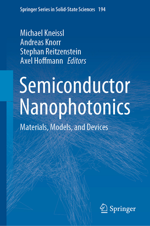
Semiconductor Nanophotonics (eBook)
XXIII, 556 Seiten
Springer International Publishing (Verlag)
978-3-030-35656-9 (ISBN)
This book provides a comprehensive overview of the state-of-the-art in the development of semiconductor nanostructures and nanophotonic devices. It covers epitaxial growth processes for GaAs- and GaN-based quantum dots and quantum wells, describes the fundamental optical, electronic, and vibronic properties of nanomaterials, and addresses the design and realization of various nanophotonic devices. These include energy-efficient and high-speed vertical cavity surface emitting lasers (VCSELs) and ultra-small metal-cavity nano-lasers for applications in multi-terabus systems; silicon photonic I/O engines based on the hybrid integration of VCSELs for highly efficient chip-to-chip communication; electrically driven quantum key systems based on q-bit and entangled photon emitters and their implementation in real information networks; and AlGaN-based deep UV laser diodes for applications in medical diagnostics, gas sensing, spectroscopy, and 3D printing.
The experimental results are accompanied by reviews of theoretical models that describe nanophotonic devices and their base materials. The book details how optical transitions in the active materials, such as semiconductor quantum dots and quantum wells, can be described using a quantum approach to the dynamics of solid-state electrons under quantum confinement and their interaction with phonons, as well as their external pumping by electrical currents. With its broad and detailed scope, this book is indeed a cutting-edge resource for researchers, engineers and graduate-level students in the area of semiconductor materials, optoelectronic devices and photonic systems.
Michael Kneissl is the Executive Director of the Institute of Solid State Physics and chair of Experimental Nanophysics and Photonics at the Technical University of Berlin (TU Berlin), Germany. He holds a dual appointment at the Ferdinand-Braun-Institute (FBH) in Berlin, where he heads the Joint Lab GaN Optoelectronics and is also spokesperson of the Collaborative Research Center 'Semiconductor Nanophotonics' (CRC 787). His interests include group III-nitride semiconductor materials, metal organic vapor phase epitaxy of wide bandgap semiconductors and nanostructures as well as novel optoelectronic devices, including UV LEDs and laser diodes. He has co-authored over 300 publications, five book chapters, and holds more than 60 patents in the area of group II-nitride device technologies. He recently co-edited a book on 'III-Nitride Ultraviolet Emitters - Technology & Applications' which was published in 2016 within the Springer Series on Material Science. In 2016 Michael Kneissl was named Fellow of the Institute of Electrical and Electronics Engineers (IEEE) for his contributions to the development of wide bandgap semiconductor laser diodes and ultraviolet LEDs.
Andreas Knorr works in the field of nonlinear optics and quantum electronics of nanostructured solids. His research is focused on the interaction of light and matter, self-consistent solutions of Maxwell- and material equations and many body effects in open quantum systems. Since 2000 Andreas Knorr holds a professorship at the TU Berlin. His scientific career, which started at the Friedrich-Schiller-University Jena led him to the Universities of New Mexico, Arizona (College of Optical Sciences), Marburg, Göttingen, Auckland, Kingston and to Sandia National Labs Albuquerque and NTT Tokio. He was a Divisional Editor of Physical Review Letters from 2013-2018.
Stephan Reitzenstein is Director of the Center of Nanophotonics of the Institute of Solid State Physics at theTU Berlin and holds the chair of Optoelectronics and Quantum Devices. His research interests focus on the development and study of nanophotonic devices and structures based on III/V semiconductor materials. Present activities include the realization of cavity-enhanced microlasers with ultra-low threshold powers, quantum-light sources for applications in advanced long-distance quantum communication and photonic circuits for on-chip quantum photonics. He has co-authored four book chapter and more than 180 publications in peer-reviewed international journals. In 2014 Stephan Reitzenstein received a prestigious EU ERC Consolidator Grant on the external quantum control of photonic semiconductor nanostructures.
Axel Hoffmann was director at the Institute of Solid State Physics and is now Guest Professor at the TU Berlin. His research expertise includes materials microcharacterization, ultra-fast phenomena in semiconductors, micro- and nanao- Raman spectroscopy, electro-optical properties in organic materials, optical properties of quantum dots, microcharacterization of organic devices, optical-properties and - gain of group-III nitrides, oxides and arsenides, spintronics, He has co-authored 545 peer reviewed publications, 102 conference papers ( 71 invited papers), 10 book chapters and 9 patents. In 2009 and 2015 he was Guest Professor at the University of Technology, Sydney, Australia.
Preface 6
Contents 9
Contributors 19
1 A Short Introduction to Semiconductor Nanophotonics 24
1.1 Nanophotonics and Internet Traffic 24
1.2 Nanophotonics and Cyber Security 27
1.3 Economic Impact of Nanophotonics 29
1.4 Semiconductor Nanophotonics 31
References 33
2 Submonolayer Quantum Dots 35
2.1 Carrier Localization in Quantum Dots 36
2.1.1 Stranski-Krastanow and Submonolayer Quantum Dots 36
2.1.2 Electronic Structure of InAs Submonolayer Quantum Dots 38
2.2 Epitaxy of Submonolayer Quantum Dots 43
2.2.1 InAs/GaAs Submonolayers 43
2.2.2 InAs/GaAs Submonolayers with Antimony 44
2.3 Atomic Structure of Submonolayer Quantum Dots 47
2.3.1 Methods for Structural Analysis 47
2.3.2 Analysis of InAs Submonolayer Depositions 49
2.3.3 Analysis of InAs Submonolayer Depositions with Antimony 53
2.4 Optical and Excitonic Properties 56
2.4.1 InAs Submonolayer Quantum-Dot Ensembles 56
2.4.2 InAs:Sb Submonolayer Quantum-Dot Ensembles 60
2.5 Devices Based on Submonolayer Quantum Dots 63
2.5.1 Gain and Efficiency 63
2.5.2 Amplitude-Phase Coupling 66
2.6 Conclusion and Perspectives 68
References 69
3 Stressor-Induced Site Control of Quantum Dots for Single-Photon Sources 74
3.1 Site-Controlled Nucleation of Quantum Dots 74
3.2 Simulation of Strain 76
3.2.1 Model for Strain Simulation 76
3.2.2 Strain in a Mesa and in a Lamella Structure 77
3.3 Nucleation Control by a Buried Aperture Stressor 80
3.3.1 Development of a Buried-Stressor Design 81
3.3.2 Proof-of-Principle for Stressor-Controlled Nucleation 83
3.3.3 Site-Control of Single Quantum Dots 84
3.4 Strain Measurement Applying Electron Holography 86
3.4.1 Reconstruction of the Strain Tensor 86
3.4.2 Phase Analysis of Dark-Field Electron Holography 88
3.4.3 Strain Analysis in a Lamella of a GaAs Mesa 90
3.5 Single-Photon Source Based on Stressor-Induced Site Control of Quantum Dots 93
3.5.1 Development of an Electroluminescence Quantum-Dot Diode 94
3.5.2 Operation Characteristics of a Single-Photon Source 95
3.5.3 Development of a Resonant-Cavity Structure 97
3.6 Realization of an Efficient Current Injection into a Single Quantum Dot 101
3.6.1 Modeling of the Current Flow in the Device 102
3.6.2 Current Confinement in pin and ppn Designs 105
3.6.3 Demonstration of a ppn QD Diode with Efficient Current Confinement 106
3.7 Conclusion and Perspectives 107
References 108
4 Coherent and Incoherent Dynamics in Quantum Dots and Nanophotonic Devices 112
4.1 Introduction 113
4.2 Ultrafast Carrier Dynamics in Semiconductors with Reduced Dimensionality 114
4.2.1 Ultrafast Gain and Phase Recovery Dynamics 115
4.2.2 Ultrafast Coherent Optical Nonlinearities 119
4.2.3 Crossed Excitons 122
4.2.4 Quantum State Tomography 126
4.3 Multisection Mode-Locked Semiconductor Lasers 129
4.3.1 Delay Differential Equation Modeling 130
4.3.2 Timing Jitter Calculation 134
4.3.3 Reducing Timing Jitter by Optical Perturbations 138
4.3.4 Tapered Multi-section Mode-Locked Laser 143
4.4 Conclusion 148
References 149
5 Optical and Structural Properties of Nitride Based Nanostructures 155
5.1 Introduction 156
5.2 Advanced Tools for Nanostructure Characterization 157
5.2.1 TEM/STEM-CL 157
5.2.2 Tip-Enhanced Raman Spectroscopy (TERS) 167
5.2.3 UV Optical and Quantum-Optical Characterization 170
5.2.4 XRD 171
5.2.5 Scanning Tunneling Microscopy and Spectroscopy (STM/STS) 177
5.3 Analysis of Nanostructure Growth in Nitrides 178
5.3.1 Growth of Nitride Based Nano- and Micro-columns 178
5.4 Optical Analysis of Low-Dimensional Nitrides 182
5.4.1 Luminescence and Composition Inhomogeneities in InGaN/GaN Micro-columns 182
5.4.2 InGaN/GaN Core-Shell Nanorods with Thick InGaN Shell 195
5.4.3 Full InGaN/GaN LED Micro-column Structures 199
5.4.4 Shielding Electric Fields in Nanowire Based Quantum-Heterostructures 205
5.4.5 Optical Properties and Charge Carrier Dynamics in 1D Quantum Wires 209
5.5 Conclusion and Perspectives 214
References 215
6 Theory of Spectroscopy and Light Emission of Semiconductors Nanostructures 222
6.1 Introduction 222
6.2 State of the Art of Microscopic Description of Quantum Dots 223
6.2.1 Quantum Dot Model 224
6.2.2 Electron-Light Interaction 225
6.2.3 Electron-Phonon Interaction 225
6.2.4 Coulomb Interaction 226
6.3 Coupled Quantum Dot-Cavity Structures 227
6.3.1 Correlation Function and Master Equation 227
6.3.2 Polarization-Entanglement 228
6.3.3 Spatial Cross Correlation of Weakly and Strongly Coupled Modes: Single, Bunched and Heralded QD Photon Sources 234
6.3.4 Effective Description of the Few and Many Emitter Limit and Application to Many Emitter Nanolasing 235
6.4 Intraband Transitions Between Bound Quantum Dot States and States of the Host Medium 238
6.4.1 Quantum Dot-Continuum Model System and Pump Probe Setup 238
6.4.2 All-Optical Reconstruction of Quantum Dot Wave Functions 239
6.4.3 Influence of Coulomb Coupling on Bound-Continuum Intraband Transitions 240
6.5 Hybrid Density Matrix Approach as a Factorization Scheme for Many-Body Systems 242
6.6 Two-Dimensional Spectroscopy in Semiconductor Nanostructures 244
6.6.1 Theory of Four-Wave Mixing Spectroscopy 244
6.6.2 Mechanisms of Coulomb Interaction in Quantum Dots 247
6.6.3 Phase-Referenced 2D Spectroscopy of Coherently Coupled Individual QDs 248
6.6.4 Förster and Dexter Transfer Processes in Coupled Nanostructures 250
6.6.5 Localization Dynamics of Excitons in Disordered Semiconductor Quantum Wells 253
6.7 Conclusion 254
References 255
7 Multi-dimensional Modeling and Simulation of Semiconductor Nanophotonic Devices 260
7.1 Introduction 261
7.2 Basic Concepts 261
7.2.1 Electronic Transport 263
7.2.2 Optical Fields 266
7.2.3 Thermodynamics 268
7.3 Quantum Dot Based Light-Emitting Devices 268
7.3.1 Quantum Dot Lasers 269
7.3.2 Single-Photon Sources 273
7.4 Numerical Methods 280
7.4.1 Numerical Methods for the Drift-Diffusion Equations 280
7.4.2 Finite-Element Approach to Maxwell's Equations 285
7.5 Applications 289
7.5.1 Quantum Dot Single-Photon Sources 289
7.5.2 Vertical-Cavity Surface-Emitting Lasers 291
7.5.3 Grating Couplers 292
7.5.4 Efficient Current Injection into Oxide-Confined Pn-Diodes 293
7.6 Conclusion and Outlook 294
References 295
8 Deterministic Quantum Devices for Optical Quantum Communication 303
8.1 Introduction 303
8.2 Numerical Modeling and Optimization of Quantum Devices for the Generation and Distribution of Single Photons 306
8.2.1 A Setup for a QD-Based Fiber-Coupled Single-Photon Source 306
8.2.2 Numerical Method for the Efficient Simulation of Optical Devices with Embedded QDs 306
8.2.3 Numerical Optimization of the Light Extraction from a Single-Photon Source 309
8.2.4 Numerical Simulation of a QD-Based Single-Photon Emitting Diode—The Role of Electrical Carrier Injection 312
8.3 Deterministic Fabrication Technologies 318
8.3.1 Ex-situ Schemes 320
8.3.2 In-situ Schemes 320
8.4 Quantum Light Sources Based on Deterministic Quantum Dot Microlenses 326
8.4.1 Microlenses for Enhanced Photon Extraction 326
8.4.2 Description of Sample Templates and Spectroscopic Techniques 328
8.4.3 Device Yield and Photon-Extraction Efficiency 329
8.4.4 Verification of Single-Photon Emission 331
8.4.5 Generation of Indistinguishable Photons 335
8.4.6 Demonstration of a Twin-Photon Source 340
8.4.7 Generation of Polarization-Entangled Photon Pairs 344
8.4.8 Strain Tuning of the Emission Energy 353
8.4.9 Quantum Dot Single-Photon Sources Emitting at Telecom Wavelength 356
8.5 On-Chip Quantum Circuits with Deterministically-Integrated Quantum Dots 362
8.5.1 Fabrication of Monolithic Waveguide Structures and an On-Chip HBT Circuit 362
8.6 Conclusion and Outlook 366
References 368
9 Quantum Networks Based on Single Photons 378
9.1 Introduction 378
9.2 Single-Photon Generation and Manipulation 380
9.2.1 Properties of Single Photons in Quantum Networks 380
9.2.2 Semiconductor Single-Photon Sources 382
9.3 Frequency Conversion of Quantum Light 383
9.3.1 Nonlinear Quantum-Optics 384
9.3.2 Conversion of Photons in the Telecom Band 385
9.3.3 Conversion of Photons from a Single Quantum Dot 385
9.4 Single-Photon Storage 387
9.4.1 Concepts of Photon Storage 387
9.4.2 Atomic Gas Cells 389
9.4.3 Interfacing Quantum Dots and Atomic Vapors 390
9.4.4 Single-Photon Storage 391
9.5 Quantum Communication 392
9.5.1 Quantum Key Distribution (QKD) Protocols 392
9.5.2 The Time-Frequency (TF-) Protocol 394
9.5.3 Numerical Studies, Higher Alphabets and Security Issues 396
9.6 Free-Space Quantum Link 397
9.6.1 Free Space QKD Transmission 397
9.6.2 Experimental Implementation of a Quantum Testbed 399
9.6.3 Evaluation and Improvements 400
9.7 Conclusion and Outlook 401
References 402
10 Vertical Cavity Surface Emitting Laser Diodes for Communication, Sensing, and Integration 408
10.1 Introduction 408
10.2 VCSEL Experimental Structures 412
10.3 VCSEL Processing, Geometric Variations, and Characterization 414
10.4 Reduced Vertical Dimension VCSELs 419
10.5 High Modulation Bandwidth VCSELs 425
10.6 VCSELs for Higher Power 431
10.7 VCSEL Arrays 435
10.8 Conclusion and Outlook 440
References 441
11 VCSEL-Based Silicon Photonic Interconnect Technologies 444
11.1 Modern Interconnect Technologies and Requirements 444
11.1.1 Classification of Interconnects 445
11.1.2 Road to Coherent Data Center Interconnects 446
11.1.3 On the Importance of Quantum Dot Lasers for Silicon Photonics 448
11.2 Long-Wavelength VCSELs 448
11.2.1 Device Structure 449
11.2.2 Operation Characteristics 450
11.3 Characterization of 1.33 µm and 1.55 µm InP VCSELs for Coherent Interconnects 452
11.3.1 Intrinsic Linewidth 454
11.4 Modeling of VCSEL-Based Coherent Interconnects 456
11.4.1 Coherent Transmission Techniques 456
11.4.2 Digital Signal Processing 457
11.4.3 Performance of VCSEL-Based Transmission Links for QPSK 457
11.5 VCSEL-Based PAM-4 Transmission Link 459
11.5.1 Setup 459
11.5.2 System Performance 460
11.6 VCSEL-Based QPSK Transmission Link 461
11.6.1 Setup 461
11.6.2 System Performance 463
11.7 Conclusion 465
References 466
12 Nitride Microcavities and Single Quantum Dots for Classical and Non-classical Light Emitters 469
12.1 Introduction 469
12.2 Bragg Mirrors in the Visible to Deep UV Spectral Region 470
12.3 Microstructure and Emission Properties of Blue/Violet Emitting III-Nitride Microcavities 474
12.3.1 Electric Fields Within AlGaN/AlInN DBRs 477
12.3.2 Plastic Relaxation of 62-Fold InGaN Multiple Quantum Wells in a GaN Cavity 478
12.3.3 Carrier Localization in a Pseudomorphically Grown InGaN MQW/DBR Structure 483
12.3.4 Local Properties of Excitonic and Photonic Modes in Violet Emitting Microcavities 485
12.4 GaN Quantum Dots: Formation, Optical and Electronic Properties 489
12.4.1 GaN Quantum Dot Formation Mechanism 491
12.4.2 Quantum Dot Emission from GaN Islands Formed at Threading Dislocations 493
12.4.3 Exciton-Phonon Coupling 500
12.4.4 Spectral Diffusion of Excitonic Complexes 503
12.4.5 Photon Statistics of the Biexciton Cascade 504
12.4.6 Unconventional Biexciton States 507
12.4.7 Monolithic Deep UV Bragg Mirrors for GaN QD Microcavities 509
12.5 Towards Electrically Driven Microcavity Devices 513
12.6 Conclusion and Perspectives 515
References 516
13 Group III-Nitride-Based UV Laser Diodes 521
13.1 Introduction 521
13.2 State-of-the-Art in Group III-Nitride Laser Diode Technologies 523
13.2.1 Near UV and Blue Laser Diodes 523
13.2.2 Optically Pumped Deep UV Lasers 524
13.2.3 Electron Beam Pumping of UV Emitters 525
13.2.4 AlGaN-Based Deep UV Laser Diodes 526
13.3 Design of AlGaN-Based Deep UV Laser Diodes 527
13.3.1 Separate Confinement Heterostructure 527
13.3.2 Design Rules for Deep UV Laser Heterostructures 528
13.3.3 Investigated Deep UV Laser Structures 530
13.4 Fabrication of AlGaN-Based UV Laser Diodes 531
13.4.1 Low Resistance Ohmic Contacts to n-AlGaN Layer 531
13.5 Low Defect Density AlN Templates 534
13.5.1 Substrates and Templates for AlGaN UV Lasers 534
13.5.2 Bulk AlN Substrates 535
13.5.3 SiC Substrates 536
13.5.4 Sapphire Substrates 536
13.6 Growth of AlGaN Laser Heterostructures 539
13.6.1 Pseudomorphic Growth of AlGaN and Critical Layer Thickness 539
13.6.2 Si- and Mg-Doping of AlGaN Materials and Superlattices 541
13.6.3 Growth and Optical Properties of AlGaN Quantum Wells 543
13.7 Gain and Losses in Deep UV AlGaN Lasers by Optical Pumping 545
13.7.1 Optical Pumping for Lasing Threshold and Gain Measurements 545
13.7.2 Optical Gain in Dependence of the Emission Wavelength 546
13.7.3 Optical Polarization and Valence Band Ordering 548
13.7.4 Loss Mechanisms in Deep UV Lasers 549
13.8 Development of Current Injection Deep UV Laser Diodes 553
13.8.1 Low Resistance n-AlGaN Current Spreading Layers 553
13.8.2 Mg-Doped AlGaN Short Period Superlattices 553
13.8.3 Efficient Carrier Injection and Carrier Confinement in Deep UV AlGaN LDs by Electron Blocking Heterostructures 556
13.8.4 Efficient Carrier Injection in Deep UV AlGaN LD by Tunnel Heterojunctions 557
13.8.5 High Density Pulsed Current Injection in UV Laser Diodes 559
13.9 Conclusion and Outlook 559
References 560
Index 565
| Erscheint lt. Verlag | 10.3.2020 |
|---|---|
| Reihe/Serie | Springer Series in Solid-State Sciences | Springer Series in Solid-State Sciences |
| Zusatzinfo | XXIII, 556 p. 374 illus., 337 illus. in color. |
| Sprache | englisch |
| Themenwelt | Naturwissenschaften ► Physik / Astronomie ► Atom- / Kern- / Molekularphysik |
| Technik ► Elektrotechnik / Energietechnik | |
| Schlagworte | electrically driven quantum key systems • energy efficient VCSEL • epitaxial growth of quantum dots • high-speed VCSEL • nanoscale photonic devices • nanostructured semiconductors • optoelectronic devices • self-consistent solution of Maxwell's equations • UV laser diode for medical applications |
| ISBN-10 | 3-030-35656-6 / 3030356566 |
| ISBN-13 | 978-3-030-35656-9 / 9783030356569 |
| Haben Sie eine Frage zum Produkt? |
Größe: 74,8 MB
DRM: Digitales Wasserzeichen
Dieses eBook enthält ein digitales Wasserzeichen und ist damit für Sie personalisiert. Bei einer missbräuchlichen Weitergabe des eBooks an Dritte ist eine Rückverfolgung an die Quelle möglich.
Dateiformat: PDF (Portable Document Format)
Mit einem festen Seitenlayout eignet sich die PDF besonders für Fachbücher mit Spalten, Tabellen und Abbildungen. Eine PDF kann auf fast allen Geräten angezeigt werden, ist aber für kleine Displays (Smartphone, eReader) nur eingeschränkt geeignet.
Systemvoraussetzungen:
PC/Mac: Mit einem PC oder Mac können Sie dieses eBook lesen. Sie benötigen dafür einen PDF-Viewer - z.B. den Adobe Reader oder Adobe Digital Editions.
eReader: Dieses eBook kann mit (fast) allen eBook-Readern gelesen werden. Mit dem amazon-Kindle ist es aber nicht kompatibel.
Smartphone/Tablet: Egal ob Apple oder Android, dieses eBook können Sie lesen. Sie benötigen dafür einen PDF-Viewer - z.B. die kostenlose Adobe Digital Editions-App.
Zusätzliches Feature: Online Lesen
Dieses eBook können Sie zusätzlich zum Download auch online im Webbrowser lesen.
Buying eBooks from abroad
For tax law reasons we can sell eBooks just within Germany and Switzerland. Regrettably we cannot fulfill eBook-orders from other countries.
aus dem Bereich


