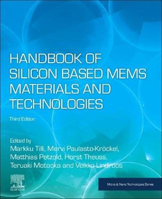
Handbook of Silicon Based MEMS Materials and Technologies
Elsevier Science Publishing Co Inc (Verlag)
978-0-12-817786-0 (ISBN)
The third edition of this book provides an important up-to-date overview of the current and emerging technologies in MEMS making it a key reference for MEMS professionals, engineers, and researchers alike, and at the same time an essential education material for undergraduate and graduate students.
Markku Tilli obtained a degree in Materials Science (Physical Metallurgy) at Helsinki University of Technology (HUT) in 1974. Until 1980 he had various research and teaching positions at HUT specializing in crystal growth technologies. From 1981 to 1984 he managed process research and development in Silicon project at HUT silicon wafer manufacturing pilot plant. Since 1985 he has had various managing positions at Okmetic in research, development and customer support areas, and held a position of Senior Vice President, Research until his retirement in 2018. His MEMS related activities started in 1982 when he developed a process to make double side polished silicon wafers for bulk micromachined sensors. Since then he has developed advanced new silicon wafer types for MEMS, including special epitaxial wafers, SOI and SOI wafers with buried cavities. His publication topics include oxygen precipitation in silicon, silicon crystal growth, wafer cleaning as well as silicon wafer manufacturing technologies and applications in MEMS. He is member of the Technology Academy of Finland and has received the honorary degree of Doctor of Science in Engineering from Aalto University. Dr. Mervi Paulasto-Kröckel is professor at Aalto University School of Electrical Engineering in Finland. She studied materials science and semiconductor technology in Helsinki University of Technology, and gradudated as MSc Tech in 1990. She continued her studies in the Technical Universities of Aachen (RWTH Aachen) and Helsinki and attained her doctoral degree in 1995. After a 2-years post-doctoral appointment at the Joint Research Centre of European Commission in the Netherlands, her professional career continued in the electronics industry. She was a Staff Principal Engineer at Motorola Semiconductor Products Sector in Munich. In 2004 Paulasto-Kröckel joined Infineon Technologies where she was the Director Package Development responsible for semiconductor assembly and interconnect development for automotive products worldwide. At the end of 2018 Dr. Paulasto-Kröckel became a professor at Helsinki University of Technology, which is now called Aalto University after a merger with two other leading universities in the Helsinki area. Her current research focus is on advanced materials and interconnect technologies for MEMS/NEMS and power electronics, as well as multi-material assemblies behavior under different loads and their characteristic failure mechanisms. Her group has extensive experience in studying interactions and interfacial reactions between dissimilar materials, such as different oxide and nitride materials, metals and semiconductors. The group has developed a combined methodology approach to solve multi-materials compatibility issues in microelectronics and microsystems. Prof. Paulasto-Kröckel has over 110 international publications in the fields of microelectronics packaging and interfacial compatibility of dissimilar materials. She is IEEE EPS Distinguished Lecturer and a member of the Finnish Academy of Technical Sciences. Matthias Petzold is Professor, Fraunhofer Institute for Microstructure of Materials and Systems IMWS, Germany. His research focuses on physical failure analysis of semiconductor materials, on strength and reliability properties of MEMS, on material diagnostics in microelectronics packaging and on innovative methods and instrumentation for microstructure diagnostics and mechanical testing. He is currently heading the institute’s Center for Applied Microstructure Diagnostics (CAM) and is deputy director of the Fraunhofer institute for Microstructure of Materials and Systems IMWS in Halle. Horst Theuss is Lead Principal, Infineon Technologies AG, Germany, where he is today responsible for Backend predevelopments focusing on new packages for MEMS and sensors. Since 2000, he has worked on a variety of assembly technologies and concepts in the field of discrete semiconductors, wafer level packaging, cavity packaging, materials and integration concepts. Teruaki Motooka received PhD degree in 1981 in Applied Physics from Kyushu University. He was a research scientist in the Central Research Laboratory, Hitachi Ltd. for 1971-1984, a visiting research assistant professor at University of Illinois at Urbana-Champaign, USA for 1984-1988, an associate professor in the Institute of Applied Physics at University of Tsukuba, Japan for 1988-1993, and became a full professor at Kyushu University in 1993. He retired from Kyushu University in 2010. He has published more than 150 scientific papers on various international journals and these papers have been cited more than 2000 times. Veikko Lindroos is Professor Emeritus, Physical Metallurgy and Materials Science, Aalto University, Finland. His research covers a broad spectrum of materials science and technology, such as metallic materials, silicon technology and MEMS materials magnetic, electronic and composite materials as well as shape memory effect and materials.
Part I 1. Properties of silicon; Fracture toughness 2. Czochralski Growth of Silicon Crystals 3. Properties of Silicon Crystals 4. Silicon Wafers: Preparation and Properties; Modern technologies 5. Epi Wafers: Preparation and Properties 6. Thin Films on Silicon 7. Thick-Film SOI Wafers: Preparation and properties
Part II 8. Multiscale Modeling Methods 9. Mechanical Properties of Silicon Microstructures 10. Electrostatic and RF-Properties of MEMS Structures 11. Optical Modeling of MEMS 12. Modeling of Silicon Etching 13. Gas Damping in Vibrating MEMS Structures 14. Recent Progress in Large-scale Electronic State Calculations and Data-driven Sciences
Part III 15. MEMS Lithography 16. Deep Reactive Ion Etching; update 17. Wet Etching of Silicon 18. Porous Silicon Based MEMS 19. Surface Micromachining 20. Vapor Phase Etch Processes for Silicon MEMS 21. Inkjet Printing, Laser-Based Micromachining and Micro 3D Printing Technologies for MEMS 22. Microfluidics and BioMEMS in Silicon
Part IV 23. Silicon Direct Bonding 24. Anodic Bonding 25. Glass Frit Bonding 26. Metallic Alloy Seal Bonding 27. Emerging Wafer Bonding Technologies 28. Bonding of CMOS Processed Wafers 29. Wafer-Bonding Equipment 30. Encapsulation by Film Deposition 31. Dicing of MEMS Devices 32. 3D Integration of MEMS 33. Own chapter for eWLP 34. Through-Substrate Via Technologies for MEMS 35. Outgassing and Gettering
Part V 36. Silicon Wafer and Thin Film Measurements 37. Oxygen and Bulk Microdefects in Silicon 38. Optical Measurement of Static and Dynamic Displacement in MEMS 39. MEMS Residual Stress Characterization: Methodology and Perspective 40. Microscale deformation analysis 41. Strength of Bonded Interfaces 42. Hermeticity Tests 43. MEMS testing and calibration 44. MEMS Reliability
Part VI 45. Case Accelerometer 46. Case Gyroscope 47. Case Pressure Sensor 48. Case Microphone 49. Case Micromirror 50. Case Optical MEMs
| Erscheinungsdatum | 24.04.2020 |
|---|---|
| Reihe/Serie | Micro & Nano Technologies |
| Sprache | englisch |
| Maße | 216 x 276 mm |
| Gewicht | 2670 g |
| Themenwelt | Technik ► Maschinenbau |
| ISBN-10 | 0-12-817786-1 / 0128177861 |
| ISBN-13 | 978-0-12-817786-0 / 9780128177860 |
| Zustand | Neuware |
| Haben Sie eine Frage zum Produkt? |
aus dem Bereich


