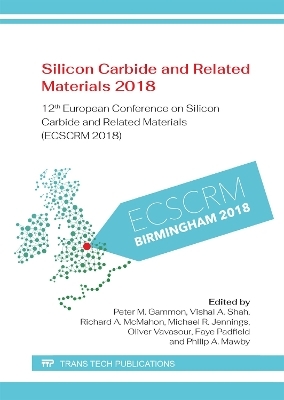
Silicon Carbide and Related Materials 2018
Trans Tech Publications Ltd (Verlag)
978-3-0357-1332-9 (ISBN)
- Titel nicht im Sortiment
- Artikel merken
Selected, peer reviewed papers from the European Conference on Silicon Carbide and Related Materials (ECSCRM 2018), September 2-6, 2018,Birmingham, UK
This volume contains selected papers from the 12th European Conference on Silicon Carbide and Related Materials (ECSCRM 2018), held in Birmingham, UK, in September 2018. Researchers discussed the latest progress in the field of silicon carbide semiconductors, including their development and production, and their application in the power electronic devices. The papers address silicon carbide growth, including bulk, epitaxial, and thin film growth; theory and characterization, including fundamentals and material properties, point and extended defects, and surfaces and interfaces; processing, focusing on doping, implantation, and contact, dielectric growth and characterization, and etching and machining; devices, including diodes, power MOSFETs, JFETs and IGBTs; reliability, circuits and applications. The contributors are academics and industrialists from around the world.
Preface
Chapter 1: Bulk and Epitaxial Growth
1.1: Physical Vapor Transport Growth
Advances in In Situ SiC Growth Analysis Using Cone Beam Computed Tomography
Cold Split Kerf-Free Wafering Results for Doped 4H-SiC Boules
Tracking of the Growth Interface during PVT-Growth of SiC Boules Using a X-Ray Computed Tomography Setup
Modified Hot-Zone Design for Large Diameter 4H-SiC Single Crystal Growth
Impacts of TaC Coating on SiC PVT Process Control and Crystal Quality
Major Carrier Element Concentrations in SiC Powder and Bulk Crystal
Variation of Vanadium Incorporation in Semi-Insulating SiC Single Crystals Grown by PVT Method
Study on N and B Doping by Closed Sublimation Growth Using Separated Ta Crucible
Polytype Control by Pretreatment of SiC Source Powder for 4H-SiC Single Crystal Growth
Optimization of the SiC Powder Source Size Distribution for the Sublimation Growth of Long Crystals Boules
New Materials for Semi-Insulating SiC Single Crystal Growth by PVT Method
A Comparative Study of the Crystal Growth Techniques of Silicon Carbide, Technology Adaption and the Road to Low Cost Silicon Carbide Materials
Research on the Key Problems in the Industrialization of SiC Substrate Materials
Influence of Dopant Concentration on Dislocation Distributions in 150mm 4H SiC Wafers
Study on Dislocation Behaviors during PVT Growth of 4H-SiC
1.2: Solution Growth
Application of Defect Conversion Layer by Solution Growth for Reduction of TSDs in 4H-SiC Bulk Crystals by PVT Growth
Effect of Melt-Back Process on the Quality of Grown Crystal in SiC Solution Growth
Evaluation of Basal Plane Dislocation Behavior in the Epitaxial Layer on a 4H-SiС Wafer Fabricated by the Solution Growth Method
Solution Growth of 4-Inch Diameter SiC Single Crystal Using Si-Cr Based Solvent
1.3: Epitaxial Growth
High Quality 4H-SiC Epitaxial Layer by Tuning CVD Process
Continuous Growth of Buffer/Drift Epitaxial Stack Based on 4H-SiC by Quick Change of N2 Flow Rate under High Growth Rate Condition
Repeatability of Epitaxial Growth of n-Type 4H-SiC Films by High Speed Wafer Rotation Vertical CVD Tool
Extensive 99% Killer Defect Free 4H-SiC Epitaxial Layer toward High Current Large Chip Devices
Influence of Substrate Properties on the Defectivity and Minority Carrier Lifetime in 4H-SiC Homoepitaxial Layers
Basal Plane Dislocation Conversion Enhancement in 4H-SiC Homo-Epitaxial Layers by Ion Implantation into the Wafer
Effect of Surface Etching Conditions on Stacking Faults in 4H-SiC Epitaxy
New SiC Epitaxial Growth Process with up to 100% BPD to TED Defect Conversion on 150mm Hot-Wall CVD Reactor
Germanium Incorporation in Silicon Carbide Epitaxial Layers Using Molecular Beam Epitaxy on 4H-SiC Substrates
A Study of CVD Growth Parameters to Fill 50-μm-Deep 4H-SiC Trenches
Effect of HCL on Surface Free Energy of SiC during CVD Trench Filling
High Temperature SiC Reactor Cleaning Using Chlorine Trifluoride Gas Achieved by Purified Pyrolytic Carbon Coating Film
1.4: 3C-Sic and Related Materials
Vapor Growth of 3C-SiC Using the Transition Layer of 3C-SiC on Si CVD Templates
Novel Carbon Treatment to Create an Oriented 3C-SiC Seed on Silicon
Modeling of the PVT Growth Process of Bulk 3C-SiC - Growth Process Development and Challenge of the Right Materials Data Base
Structural Strain in Single Layer Graphene Fabricated on SiC
Chapter 2: Characterisation
2.1: Characterisation of the SiC-Oxide Interface
Evaluation of the Impact of Al Atoms on SiO2/ SiC Interface Property by Using 4H-SiC n+-Channel Junctionless MOSFET
Cryogenic Characterization of NH3 Post Oxidation Annealed 4H-SiC Trench MOSFETs
Surface Morphology of 4H-SiC after Thermal Oxidation
Subthreshold Drain Current Hysteresis of Planar SiC MOSFETs
Accurate Dopant and Interface Characterization in Oxidized SiC with Refined Non-Contact C-V Technique
First Principles Study of the Influence of the Local Steric Environment on the Incorporation and Migration of NO in a-SiO2
Evidence for an Abrupt Transition between SiO2 and SiC from EELS and Ab Initio Modelling
Theory of Carbon-Vacancy Diffusion at the SiO2/4H-SiC Interface
DFT Calculation for Oxidation Reaction of SiC(0001)
Characterization of SiO2/SiC Near-Interface Oxide Traps with Constant-Capacitance Deep-Level Transient Spectroscopy
Characterization of Near-Interface Traps at Dielectric/SiC Interfaces Using CCDLTS
Atomic Coordination Analysis of Nitrogen Introduced in SiO2/ SiC Interface and SiO2 Layer by XAFS Measurement
Sub-nm-Scale Depth Profiling of Nitrogen in NO- and N2-Annealed SiO2/4H-SiC(0001) Structures
SiO2/SiC MOSFETs Interface Traps Probed by Nanoscale Analyses and Transient Current and Capacitance Measurements
A Temperature Independent Effect of Near-Interface Traps in 4H-SiC MOS Capacitors
Identification of Near-Interface Trap Distribution by Parameter Estimation
Impact of Pit Defects on the Initial Electrical Characteristics of Planar-MOSFET Devices
2.2: Extended and Surface Defects
Observation of Dislocation Conversion in 4H-SiC Epitaxial Wafer by Mirror Projection Electron Microscopy
Monitoring of Substrate and Epilayer Surfaces by Mirror Projection Electron Microscope
Optical Discrimination of TSDs and TEDs in 4H-SiC Substrates and Epitaxial Layers by Phase Contrast Microscopy Method
Dynamics Analysis of Single Shockley Stacking Fault Expansion in 4H-SiC P-i-N Diode Based on Free Energy
Analysis of Basal Plane Dislocation Dynamics in 4H-SiC Crystals during High Temperature Treatment
Detecting Basal Plane Dislocations Converted in Highly Doped Epilayers
Dislocations Propagation Study Trough High-Resolution 4H-SiC Substrate Mapping
Initiation of Shockley Stacking Fault Expansion in 4H-SiC P-i-N Diodes
Effect of Defects in Silicon Carbide Epitaxial Layers on Yield and Reliability
Evaluation of Effect of Mechanical Stress on Stacking Fault Expansion in 4H-SiC P-i-N Diode
2.3: Characterisation of SiC Polytypes
Deep Electronic Levels in n-Type and p-Type 3C-SiC
Combined EPR and Photoluminescence Study of Electron and Proton Irradiated 3C-SiC
Effects of Aluminum Incorporation on the Young’s Modulus of 3C-SiC Epilayers
Electrically Active Levels Generated by Long Oxidation Times in 4H-SiC
Minority Carrier Lifetime Measurements on 4H-SiC Epiwafers by Time-Resolved Photoluminescence and Microwave Detected Photoconductivity
Carrier Transport Mechanisms in Ion Implanted and Highly-Doped p-Type 4H-SiC(Al)
Relationship between Temperature Dependencies of Resistivity and Hall Coefficient in Heavily Al-Doped 4H-SiC Epilayers
4H-SiC p-Type Doping Determination from Secondary Electrons Imaging
Ultra-Fast and High-Precision Crystal Orientation Measurements on 4H-SiС
Study of Nitrogen Doping Effect on Lattice Strain Variation in 4H-SiC Substrates by Synchrotron X-Ray Contour Mapping Method
Newly Resolved Phonon-Assisted Transitions and Fine Structure in the Low Temperature Wavelength Modulated Absorption and Photoluminescence Spectra of 6H SiC
High Resolution Investigation of Stacking Fault Density by HRXRD and STEM
2.4: New SiC Material Functionality
Electrical Characterisation of Thick 3C-SiC Layers Grown on Off-Axis 4H-SiC Substrates
Nano and Micro-Scale Simulations of Si/4H-SiC and Si/3C-SiC NN-Heterojunction Diodes
Characterization of β-Silicon Carbide and Potential Use as Irradiation Temperature Monitor
Terahertz Emission from SiC Natural Superlattices in Strong Electrical Field
Chapter 3: Processing
3.1: Ion Implantation
Recent Advances in the Doping of 4H-SiC by Channeled Ion Implantation
Channeled Implantations of p-Type Dopants into 4H-SiC at Different Temperatures
Channeling in 4H-SiC from an Application Point of View
Fabrication and Characterization of 3.3-kV SiC DMOSFET with Self-Aligned Channels Formed by Tilted Ion Implantation
Comparison of Ranges for Al Implantations into 4H-SiC (0001) Using Channeled Ions and an Ion Energy in the Bethe-Bloch Region
Thermal Annealing of High Dose P Implantation in 4H-SiC
High-Concentration, Low-Temperature, and Low-Cost Excimer Laser Doping for 4H-SiC Power Device Fabrication
Effects of Thermal Annealing Processes in Phosphorous Implanted 4H-SiC Layers
Increasing Laser-Doping Depth of Al in 4H-SiC by Using Expanded-Pulse Excimer Laser
Activation Energy for the Post Implantation Annealing of 1019 cm-3 and 1020 cm-3 Ion Implanted Al in 4H SiC
1300°C Annealing of 1×10²⁰ Al+ Ion Implanted 3C-SiC
Raman Spectroscopy Characterization of Ion Implanted 4H-SiC
Surface Characterization of Ion Implanted 4H-SiC Epitaxial Layers with Ion Energy and Concentration Variations
On the Origin of Charge Compensation in Aluminum-Implanted n-Type 4H-SiC by Analysis of Hall Effect Measurements
Lateral Straggling of Ion Implantation Distributions in 4H-SiC Investigated by SIMS
Decoration of Al Implantation Profiles in 4H-SiC by Bevel Grinding and Dry Oxidation
Determination of Compensation Ratios of Al-Implanted 4H-SiC by TCAD Modelling of TLM Measurements
3.2: SiC-Oxide Interface Processing
Characterization of Ba-Introduced Thin Gate Oxide on 4H-SiC
Study of the Post-Oxidation-Annealing (POA) Process on Deposited High-Temperature Oxide (HTO) Layers as Gate Dielectric in SiC MOSFET
Electrical Characterization of MOCVD Grown Single Crystalline AlN Thin Films on 4H-SiC
Improved SiO2/ 4H-SiC Interface Defect Density Using Forming Gas Annealing
Improved Field Effect Mobility in Si-Face 4H-SiC MOSFETs with a Deposited SiNx Interface Layer
Evidence of Channel Mobility Anisotropy on 4H-SiC MOSFETs with Low Interface Trap Density
Electrical Properties of Thermal Oxide on 3C-SiC Layers Grown on Silicon
3.3: Contacts and Other Processing
Fabrication and Characterization of Ohmic Contacts to 3C-SiC Layers Grown on Silicon
Comparison between Ni-SALICIDE and Self-Aligned Lift-Off Used in Fabrication of Ohmic Contacts for SiC Power MOSFET
Microstructural Analysis of Ti/Ni Bilayer Ohmic Contacts on 4H-SiC Layers
Optimization of Ni/Nb Ratio for High-Temperature-Reliable Ni/Nb Silicide Ohmic Contact on 4H-SiC
Laser Annealing Simulations of Metallisations Deposited on 4H-SiC
Argon Bombardment of 4H Silicon Carbide Substrates for Tailored Schottky Diode Barrier Heights
Surface Effects of Passivation within Mo/4H-SiC Schottky Diodes through MOS Analysis
Deep Level Transient Spectroscopy (DLTS) Study of 4H-SiC Schottky Diodes and PiN Diodes
Chlorine Trifluoride Gas Distributor Design for Single-Crystalline C-Face 4H-Silicon Carbide Wafer Etcher
High-Efficiency Planarization of SiC Wafers by Water-CARE (Catalyst-Referred Etching) Employing Photoelectrochemical Oxidation
Impact of Subsurface Damage on SiC Wafer Shape
Chapter 4: Devices and Applications
4.1: Rectifying Devices
Study of 4H-SiC Superjunction Schottky Rectifiers with Implanted P-Pillars
Surge Current and Avalanche Robustness of Commercial 1200 V SiC Schottky Diodes
Influence of Trench Design on the Electrical Properties of 650V 4H-SiC JBS Diodes
The Impact of Non-Ideal Ohmic Contacts on the Performance of High-Voltage SiC MPS Diodes
On the Development of 1700V SiC JBS Diodes in a 6-Inch Foundry
Mechanisms and Characteristics of Large-Area High-Current-Density 4H-SiC Trench Junction Barrier Schottky Diodes
Advanced Electrical Characterisation of High Voltage 4H-SiC PiN Diodes
Performance of 4H-SiC Bipolar Diodes as Temperature Sensor at Low Temperatures
Multi-Barrier Height Characterization and DLTS Study on Ti/W 4H-SiC Schottky Diode
4.2: Power MOSFET
Comparison of SiC MOSFET Characteristics Following Body-Diode Forward-Current Stress
Achieving Reduced Specific On-Resistance in 1.2 kV SiC Power MOSFETs at Elevated Temperature
Temperature Dependency of Silicon Carbide MOSFET On-Resistance Characterization and Modeling
Temperature Dependence of dV/dt Impact on the SiC-MOSFET
1.2 kV SiC Trench-Gate MOSFETs with Dual Shielding Regions
Design Optimization of 1.2kV 4H-SiC Trench MOSFET
Inverse Modeling of 4H-SiC Trench Gate MOSFETs Validated with Electrical and Physical Characterization
Suppression of Short-Channel Effects in 4H-SiC Trench MOSFETs
1.2-kV SiC Trench-Etched Double-Diffused MOS (TED-MOS)
An Investigation into the Dynamic Behavior of 3.3kV MOSFETs Body Diode
Experimental Study of High-Temperature Switching Performance of 1.2kV SiC JBSFET in Comparison with 1.2kV SiC MOSFET
Design of a 4H-SiC RESURF n-LDMOS Transistor for High Voltage Integrated Circuits
Impact of Interface Trap Density of SiC-MOSFET in High-Temperature Environment
4.3: Bipolar, JFETs and Other Switching Devices
Performance Improvement of >10kV SiC IGBTs with Retrograde p-Well
Deep Trench Termination Structure with p-Type SiC Layer for Improved Reliability of High Voltage IGBT
Improved Device Characteristics Obtained Using a Novel High-K Dielectric Stack for 4H-SiC n-IGBT: HfO2-SiO2- AlN
15 kV n-GTOs in 4H-SiC
SiC Charge-Balanced Devices Offering Breakthrough Performance Surpassing the 1-D Ron versus BV Limit
Improvement of Switching Characteristics in 6.5-kV SiC IGBT with Novel Drift Layer Structure
Simulation Study for the Structural Cell Design Optimization of 15kV SiC p-Channel IGBTs
TCAD Model Calibration of High Voltage 4H-SiC Bipolar Junction Transistors
Silicon Carbide BJT Oscillator Design Using S-Parameters
Effect of Temperature on the Electrical Characteristics of 4H-SiC Planar n/p-Type Junctionless FET: Physics Based Simulation
Compact Modeling of SiC and GaN Junction FETs at High Temperature
High-Voltage SiC-JFET Fabrication and Full Characterization
Performance Limits of Vertical 4H-SiC and 2H-GaN Superjunction Devices
First Experimental Test on Bipolar Mode Field Effect Transistor Prototype in 4H-SiC: A Proof of Concept
Development of SOI FETs Based on Core-Shell Si/SiC Nanowires for Sensing in Liquid Environments
4.4: Radiation and Quantum Devices
Creation of Color Centers in SiC PN Diodes Using Proton Beam Writing
First-Principles Study on Photoluminescence Quenching of Divacancy in 4H SiC
Radiation Effects on 1.7kV Class 4H-SiC Power Devices: Development of Compact Simulation Models
Electrophysical and Optical Properties of 4H-SiC UV Detectors Irradiated with Electrons
Direct Bonding of 4H-SiC and SOI Wafers for Radiation-Hardened Image Sensors
Dependence of the Carrier Removal Rate in 4H-SiC PN Structures on the Irradiation Temperature
Change in the Parameters of Electron-Irradiated 4H-SiC Schottky Diodes as a Function of the Time during Low-Temperature Isothermal Annealing
Impact of Device Structure on Neutron-Induced Single-Event Effect in SiC MOSFETs
4.5: Device Ruggedness and Reliability
Gate Oxide Reliability of SiC MOSFETs and Capacitors Fabricated on 150mm Wafers
Novel Method for Evaluation of Negative Bias Temperature Instability of SiC MOSFETs
1200 V SiC MOSFETs with Stable VTH under High Temperature Gate Bias Stress
Influence of High-Temperature Bias Stress on Room-Temperature VT Drift Measurements in SiC Power MOSFETs
Design Considerations for Robust Manufacturing and High Yield of 1.2 kV 4H-SiC VDMOS Transistors
Dynamic Characterization and Robustness Test of High Voltage SiC MOSFETs
Avalanche Ruggedness Characterization of 10 kV 4H-SiC MOSFETs
Avalanche Robustness of 4600 V SiC DMOSFETs
Reliability and Ruggedness of Planar Silicon Carbide MOSFETs
Capability of SiC MOSFETs under Short-Circuit Tests and Development of a Thermal Model by Finite Element Analysis
Comparative Study on the Repetitive Unclamped-Inductive-Switching Capability(R-UIS) of 1200V 160mOhm SiC Planar Gate MOSFETs
Superior Short Circuit Performance of 1.2kV SiC JBSFETs Compared to 1.2kV SiC MOSFETs
Optimization of 1700V SiC MOSFET for Short Circuit Ruggedness
Industrial and Body Diode Qualification of Gen-III Medium Voltage SiC MOSFETs: Challenges and Solutions
4.6: CMOS and Integrated Circuits
Demonstration of 4H-SiC JFET Digital ICs Across 1000°C Temperature Range without Change to Input Voltages
A Monolithic 500°C D-Flip Flop Realized in Bipolar 4H-SiC TTL Technology
A Study on Fastening the Switching Speed for Wide Bandgap Semiconductor Based Super Cascode
Improving 5V Digital 4H-SiC CMOS ICs for Operating at 400°C Using PMOS Channel Implantation
High Temperature High Current Gain IC Compatible 4H-SiC Phototransistor
4H-SiC Trench pMOSFETs for High-Frequency CMOS Inverters
SiC Vertical-Channel n- and p-JFETs Fully Fabricated by Ion Implantation
Improved Offset Voltage Stability of 4H-SiC CMOS Operational Amplifier by Increasing Gamma Irradiation Resistance
4.7: Modules and Converters
Comparative Study of Developed 1200V/50A Full SiC IEMOS and VMOS Power Module
An Efficient Simulation Methodology to Quantify the Impact of Parameter Fluctuations on the Electrothermal Behavior of Multichip SiC Power Modules
6.5 kV Si/SiC Hybrid Power Module Technology
Development of a High-Speed Switching Silicon Carbide Power Module
SiC Power Devices for Applications in Hybrid and Electric Vehicles
Power Loss Comparison in a BOOST PFC Circuit Considering the Reverse Recovery of the Forward Diode
| Erscheinungsdatum | 02.09.2019 |
|---|---|
| Reihe/Serie | Materials Science Forum |
| Zusatzinfo | Illustrations, unspecified |
| Verlagsort | Zurich |
| Sprache | englisch |
| Maße | 170 x 240 mm |
| Gewicht | 1660 g |
| Themenwelt | Technik ► Elektrotechnik / Energietechnik |
| Technik ► Maschinenbau | |
| ISBN-10 | 3-0357-1332-4 / 3035713324 |
| ISBN-13 | 978-3-0357-1332-9 / 9783035713329 |
| Zustand | Neuware |
| Haben Sie eine Frage zum Produkt? |
aus dem Bereich


