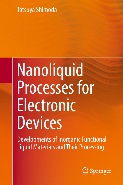
Nanoliquid Processes for Electronic Devices (eBook)
XVI, 590 Seiten
Springer Singapore (Verlag)
978-981-13-2953-1 (ISBN)
This book summarizes the results of the research on how to make small electronic devices with high properties by using simple liquid processes such as coating, self-assembling and printing, especially focusing on devices composed of silicon and oxide materials. It describes syntheses and analyses of solution materials, formations of solid thin films from solutions, newly developed patterning methods to make devices, and characterization of the developed devices.
In the first part of the book, the research on liquid silicon (Si) materials is described. Because the use of a liquid material is a quite new idea for Si devices, this book is the first one to describe liquid Si materials for electronic devices. Si devices as typified by MOS-FET have been produced by using solid and gas materials. This volume precisely describes a series of processes from material synthesis to device fabrication for those who are interested and are/will be engaged in liquid Si-related work. In the latter part of the book, a general method of how to make good oxide films from solutions and a new imprinting method to make nanosized patterns are introduced. For making oxide films with high quality, the designing of the solution is crucial. If a solution is designed properly, a gel material called 'cluster gel' can be formed which is able to be imprinted to form nanosized patterns.
The anticipated readers of this book are researchers, engineers, and students who are interested in solution and printing processes for making devices. More generally, this book will also provide guidelines for corporate managers and executives who are responsible for making strategies for future manufacturing processes.
This book summarizes the results of the research on how to make small electronic devices with high properties by using simple liquid processes such as coating, self-assembling and printing, especially focusing on devices composed of silicon and oxide materials. It describes syntheses and analyses of solution materials, formations of solid thin films from solutions, newly developed patterning methods to make devices, and characterization of the developed devices. In the first part of the book, the research on liquid silicon (Si) materials is described. Because the use of a liquid material is a quite new idea for Si devices, this book is the first one to describe liquid Si materials for electronic devices. Si devices as typified by MOS-FET have been produced by using solid and gas materials. This volume precisely describes a series of processes from material synthesis to device fabrication for those who are interested and are/will be engaged in liquid Si-related work. Inthe latter part of the book, a general method of how to make good oxide films from solutions and a new imprinting method to make nanosized patterns are introduced. For making oxide films with high quality, the designing of the solution is crucial. If a solution is designed properly, a gel material called "e;cluster gel"e; can be formed which is able to be imprinted to form nanosized patterns. The anticipated readers of this book are researchers, engineers, and students who are interested in solution and printing processes for making devices. More generally, this book will also provide guidelines for corporate managers and executives who are responsible for making strategies for future manufacturing processes.
Tatsuya ShimodaProfessor, Japan Advanced Institute of Science and Technology Member of academic society: MRS Japan Japan Society of Applied Physics (JSAP) The Japanese Sol-Gel SocietySociety for scientific committee: A member of Nanoimprint Technology Study Group in JSAP A member of Single-Nanometer Figuration and the Structure-Induced Property Study Group in JSAP
Part I Introduction to liquid process
Chapter 1. Liquid process
1-1 Liquid and its formability
1-2 Categories of liquid process
1-2-1 First step: Conversion way from liquid to solid
1-2-2 Second step: Direct forming process
Part II Silicon-based materials
Chapter 2. Guide to silicon-based materials
Chapter 3. Liquid silicon
3-1 CPS
3-1-1 Hydrosilanes and CPS
3-1-2 Structures of a CPS molecule
3-1-3 Electronic structure of isolated CPS molecule
3-1-4 Interaction between CPS molecules
3-2 Silicon ink
3-2-1 Silicon ink from CPS
3-2-2 Polymer structure in silicon ink
3-3-3 Doped silicon inks
Chapter 4. Thin film formation by coating
4-1 Coating process and molecular forces
4-2 The origin of molecular forces
4-2-1 Theory of van der Waals free energy
4-2-2 Measurement of refractive index n
4-2-3 Molecular forces of CPS and silicon compounds
4-3 Coating of Si ink
4-3-1 General remarks on Si ink coating
4-3-2 Observations of liquid films
4-3-3 Hamaker constant and coating property
4-4 Conversion from polysilane to amorphous Si by pyrolysis
4-4-1 Film appearance during pyrolysis and TG/DTA analysis of Si ink
4-4-2 Raman scattering analysis
4-4-3 FT-IR and SIMS analyses
4-4-4 Properties of amorphous films
Chapter 5. Liquid vapor deposition using liquid silicon (LVD)
5-1 Formation of i, n and p type silicon film by LVD
5-1-1 LVD method and experiment
5-1-2 CPS deposition process
5-1-3 Film properties
5-1-4 Conclusion
5-2 High-quality amorphous silicon film with LVD
5-2-1 New equipment for LVD
5-2-2 Film quality with processing temperature
5-2-3 Film quality with CPS supply speed
5-2-4 Electronic properties of a-Si:H films
5-2-5 Oxygen contamination in a-Si:H film
5-2-6 Summary
Chapter 6. Liquid silicon family materials (1)
-- SiO2, CoSi2 and Al from liquid Si --
6-1 SiO2 fabrication from liquid silicon
6-1-1 Forming SiO2 films from liquid silicon material
6-1-2 The sole solution-processed SiO2 film for TFTs
6-1-3 Multi use of solution-processed SiO2 films for TFTs
6-1-4 Conclusion
6-2 CoSi2 fabrication from liquid silicon
6-2-1 Metal silicide from solution
6-2-2 Synthesis of cobalt silicide ink
6-2-3 Formation of CoSi2 films
6-2-4 TEM observation
6-2-5 Comparison of this process with the conventional ones
6-2-6 More detailed analyses
6-2-7 Conclusions
6-3 Al fabrication via solution process
6-3-1 Triethylamine alane as a precursor of metal Al
6-3-2 Deposition process and reaction
6-3-3 Analysis of film structure and Al growth manner
6-3-4 Selective deposition of Al
6-3-5 Conclusion
Chapter 7. Liquid silicon family materials (2)
-- SiC ink and SiC film from liquid Si --
7-1 SiC fabrication via liquid process
7-1-1 Preparation and characterization of SiC precursor polymer
7-1-2 a-SiC film formation and analyses of films
7-1-3 Polymer structure
7-1-4 Polymer-to-ceramic conversion
7-1-5 Conclusion
7-2 Correlation of Si/C stoichiometry between SiC ink and a-SiC film
7-2-1 Polymer and film preparation
7-2-2 Correlation between PSH and a-SiC
7-2-3 Structural properties of an a-SiC film
7-2-4 Optical and electrical properties of an a-SiC film
7-2-5 Conclusion
7-3 n-type a-SiC by coating
7-3-1 Polymer and film preparation and their analyses
7-3-2 Polymer analysis
7-3-3 Thin-film formation
7-3-4 Effect of carbon content on film
7-3-5 Effect of phosphorous concentration on film
7-3-6 Conclusion
7-4 p-type a-SiC via LVD method
7-4-1 SiC-ink preparation and film deposition
7-4-2 Ink analysis
7-4-3 Film analysis
7-4-4 Discussion
7-4-5 Conclusion
Chapter 8. Nano pattern formation using liquid silicon
8-1 Area selective deposition of silicon family materials
8-1-1 Area selective deposition of silicon using the difference of molecular force
8-1-2 Selective deposition using the reactive difference
8-2 Beam assisted deposition of silicon
8-2-1 Free writing of silicon by FIB-CVD and advantage of CPS for a source material
8-2-2 Experimental
8-2-3 Deposition of silicon patterns
8-2-4 Characterization of the deposited patterns
8-2-5 Summary
8-3 Direct imprinting of silicon using liquid silicon
8-3-1 Nano-imprinting and silicon
8-3-2 Experimental section
8-3-3 Imprinted patterns with Mold 1
8-3-4 Influence of baking temperature on imprinting in Mold 2
8-3-5 Raman and FTIR analyses
8-3-6 Solid-phase crystallization of Si nano-patterns
8-3-7 Discussion
8-3-8 Conclusion
Chapter 9. Development of solar cells using liquid silicon
9-1 Thin film solar cells by coating
9-1-1 Solution preparation and film formation
9-1-2 Characteristics of coated films and their improvement by hydrogen radical treatment
9-1-3 Fabrication of solar cells and their properties
9-1-4 Conclusion
9-2 Thin film solar cells by LVD
9-2-1 Solar cell fabrication using LVD
9-2-2 Solar cell fabrication using the improved LVD
9-2-3 Conclusion
9-3 Application of liquid silicon for HBC type solar cells
9-3-1 Experimental procedure
9-3-2 Thermal stability of LVD a-Si passivation films
9-3-3 Storage stability of c-Si wafers passivated with LVD a-Si films
9-3-4 Feature of LVD a-Si passivation films and advantage of LVD method
9-3-5 Conclusion
Chapter 10. Development of thin film transistors using liquid silicon
10-1 Poly-Si thin film transistor (TFT)
10-1-1 Preparation of liquid silicon
10-1-2 Poly-Si TFT
10-1-3 Inkjet printing of a channel
10-1-4 Conclusion
10-1-5 Experimental methods
10-2 Single-grain Si-TFT
10-2-1 Forming single grains from liquid Si
10-2-2 Fabrication of single-grain TFTs
10-2-3 Single-grain TFTs on flexible substrates
10-2-4 Conclusion
10-3 TFT on paper
10-3-1 Poly-Si film from polysilane
10-3-2 TFT fabrication on paper
10-3-3 Properties of TFT on paper
10-3-4 Further improving as a conclusion
10-3-5 Experimental method
Part III Oxide-based materials
Chapter11. Guide to Oxide-based materials
Chapter 12. Improvement of solid through improved solutions and gels (1)
-- Utilization of Reduction agent and reduced atmosphere PZT --
12-1 Low temperature process of PZT bulk
12-1-1 Introduction and experimental
12-1-2 X-ray diffraction, TEM and XPS
12-1-3 XAFS
12-1-4 Thermal analysis
12-1-5 Discussion
12-1-6 Conclusion
12-1-7 Experimental detail
12-2 Low temperature process of PZT thin film
12-2-1 Introduction
12-2-2 Low temperature process of PZT thin film using reduced atmosphere
12-2-3 Process optimization
12-2-4 PZT film properties
12-2-5 Conclusion
12-2-6 Experimental methods
12-3 Ru and RuO thin film
12-3-1 Introduction
12-3-2 Thermal behaviors and structure of the precursor
12-3-3 Effect of amine content
12-3-4 Effects of amine structure
12-3-5 Properties of the prepared Ru0 and RuO2 thin films
12-3-6 Conclusion
12-3-7 Experimental methods
12-4 Low temperature processed RuO2 by green laser annealing
12-4-1 Introduction
12-4-2 Green laser irradiation to RuO2 precursor films
12-4-3 Resistivity of the GLA annealed films
12-4-4 Conclusion
12-4-5 Experimental methods
Chapter 13. Improvement of solid through improved solutions and gels (2)
– The other methods --
13-1Improvement of insulator property of LaZrO by amelioration of solution
13-1-1Introduction
13-1-2 Properties of Films Prepared at Temperatures between 400 °C and 600 °C
13-1-3 TG/DTA analysis.
13-1-4 Mass analysis.
13-1-5 High energy XRD analysis.
13-1-6 XAFS analysis.
13-1-7 Analysis of elemental composition for the annealed films.
13-1-8 Summary of the above analyses.
13-1-9 Conclusions
13-1-10 Experimental methods
13-2 Combustion synthesized ITO
13-2-1 SCS-ITO solutions and thin-film formation
13-2-2 Solution-processed TFTs using SCS-ITO as S&D electrodes
13-3-3 Conclusions
Chapter 14. Direct imprinting of gel (nano-Rheology Printing)
14-1 nano-Rheology Printing (n-RP) of ITO
14-1-1 Introduction to nano-Rheology Printing and its feasibility on ITO
14-1-2 Analysis of the gel material
14-1-3 Changes in the gel film during nano-Rheology Printing
14-1-4 Feature of the nano-Rheology Printing
14-1-5 Conclusion
14-1-6 Experimental details
14-2 Evaluating ITO gels via cohesive energy
14-2-1 Preparation of ITO solution and thin films
14-2-2 Conventional methods for evaluating the state of a gel
14-2-3 New methods for evaluating cohesive energy of a gel
14-2-4 Analytical results using conventional methods
14-2-5 Evaluated cohesive energies of gels
14-2-6 Conclusion
14-3 Origin of the thermal plasticity of ZrO gels
14-3-1 Introduction
14-3-2 Thermal plasticity property and rheology printing for ZrO gels
14-3-3 Structure of ZrO gels
14-3-4 Origin of thermal plasticity of Zr-gels
14-3-5 Conclusion
14-3-6 Experimental methods
14-4 nano-sized patterns of RuLaO by n-RP
14-4-1 Conversion from solutions to solids
14-4-2 Properties of nano-Rheology Printing
14-4-3 Analysis of gels and solutions
14-4-4 n-RP mechanism of Ru-La gel
14-4-5 Conclusion
14-4-6 Experimental methods
Chapter 15. Novel materials proper to liquid process
15-1 High dielectric constant BiNbO material (1) -- Bi:Nb=1:1 –
15-1-1 BiNbO materials for ceramics capacitors
15-1-2 Electrical properties of a new BiNbO material
15-1-3 Improvement of solution for a standard process of the BNO films
15-1-4 Electric properties of the films from the improved solution
15-1-5 Pyrolysis of the improved solutions and gels
15-1-6 Crystalline identification by XRD and HRTEM
15-1-7 Crystallization pathway of solution-processed BNO
15-1-8 Summary
15-1-9 Experimental details
15-2 High dielectric constant BiNbO material (2) -- Nb-rich composition --
15-2-1 Preparation of BNO precursor solution
15-2-2 Analysis of equilibrium phases appeared in the film from N50
15-2-3 Relation of the relative dielectric constant and XRD pattern with Nb content
15-2-4 Thermal analysis of N50, N60, and N67 solutions
15-2-5 Relations of the relative dielectric constant and tan δ with the annealing temperature
15-2-6 Conclusions
15-3 New p-type semiconductors
15-3-1 Introduction
15-3-2 Experimental
15-3-3 Ln-Ru(Ir)-O
15-3-4 Bi(Pb)-Ru(Ir)-O
15-3-5 Summary
Chapter 16. Thin film oxide-transistor by liquid process (1)
-- FGT :Ferroelectric Gate Thin Film Transistor --
16-1 Pt and PZT films for FGT
16-1-1 Introduction
16-1-2 Experimental procedures
16-1-3 Optimization of Pt/Ti films
16-1-4 Optimization of PZT films
16-1-5 FGT device properties and performance
16-1-6 Conclusion
16-2 All-solution-FGT Example 1
16-2-1 Introduction
16-2-2 Experimental details
16-2-3 Structural properties
16-2-4 Electrical properties
16-2-5 Conclusion
Chapter 17. Thin film oxide-transistor by liquid process (2)
-- UV and solvothermal treatments for TFT fabrication --
17-1 UV treatment for TFT
17-1-1 Introduction
17-1-2 Experimental details
17-1-3 Thermal behavior of In–Ga–Zn–O solution
17-1-4 Effect of UV/O3 treatment
17-1-5 TFT performance
17-1-6 Summary
17-2 UV treatment for all-liquid-processed TFT Example 2
17-2-1 Introduction
17-2-2 Experimental details
17-2-3 Effects of UV/O3 treatment and TFT properties
17-2-4 Compositional investigation with applying UV/O3 treatment
17-2-5 All-solution-processed TFT
17-2-6 Conclusion
17-3 UV and solvothermal treatments for TFTs
17-3-1 Introduction
17-3-2 Experimental methods
17-3-3 Formation of hybrid clusters.
17-3-4 Light absorption analysis of solutions.
17-3-5 Low-temperature UV-annealing of films and their characterization.
17-3-6 Low-temperature fabrication of transistors
17-3-7 Conclusion
17-4 Thermal-UV treatment
17-4-1 Introduction
17-4-2 Experiment details
17-4-3 Result and discussion
17-4-4 Conclusion
17-5 UV patterning for TFT fabrication
17-5-1 Introduction
17-5-2 UV irradiation and re-dissolving (UV-RD) method
17-5-3 Patterning of InO film
17-5-4 Patterning of component films for a TFT
17-5-5 TFT fabrication by the UV-RD patterning method
17-5-6 Conclusion
Chapter 18. Thin film oxide-transistor by liquid process (3)
-- High-Performance Solution-Processed ZrInZnO TFT --
18-1 ZrInZnO semiconductor film
18-1-1 Introduction
18-1-2 Experimental details
18-1-3 Film characteristics
18-1-4 TFT characteristics
18-1-5 Conclusion
18-2 ZrInZnO-TFTwith polysilazane-based SiO2 gate insulator
18-2-1 Introduction
18-2-2 Experimental details
18-2-3 Quality of SiO2 film made from polysilazane and its leakage current mechanizm
18-2-4 TFT using ZrInZnO channel and polysilazane derived SiO2
18-2-5 Conclusion
18-3 ZrInZnO-TFT by UV treatment: all-liquid-processed TFT Example 3
18-3-1 Introduction
18-3-2 Experimental details
18-3-3 Preparation of each component layer
18-3-4 Fabrication of all solution-processed TFT with high performance
18-3-5 Conclusion
18-4 All liquid-processed active matrix backplane for EPD
18-4-1 Introduction
18-4-2 Oxide films used in the AM-BP
18-4-3 Fabrication of active matrix TFT backplane (AM-TFT-BP)
18-4-4 Active matrix driven EPD panel – design, panel fabrication and driving method –
18-4-5 Performance of the TFTs and TFT-EPDs
18-4-6 Conclusion
Chapter 19. Device fabrication by n-RP
19-1 Fabrication of FGT and TFT by n-RP
19-1-1 The developed TFTs and their solutions
19-1-2 Solutions for TFT-1
19-1-3 Solutions for TFT-2
19-1-4 TFT Fabrication by nano-Rheology Printing
19-1-5 Conclusion
19-2 High-performance TFT by n-RP
19-2-1 Introduction
19-2-2 Problems of the previously developed TFT and their solutions
19-2-3 TFT structure and fabrication process
19-2-4 Shape, morphology and microstructure of the TFT by n-RP
19-2-5 Electric properties of the TFT by n-RP
19-2-6 Conclusion
19-3 Short channel TFT by n-RP
19-3-1 Introduction
19-3-2 TFT structure and its fabrication
19-3-3 Synthesis of metal oxide precursor solutions
19-3-4 LRO/Pt gate electrode pattern by the nRP
19-3-5 Sub-micron channel length by the nRP
19-3-6 Performance of sub-micron channel length nRP-oxide TFTs
19-3-7 Conclusion
19-4 Active-matrix back plane by n-RP
19-4-1 Introduction
19-4-2 TFT fabrication process and details of n-RP
19-4-3. Solution preparation and others
19-4-4 Development of alignment system for n-RP process
19-4-5 Evaluation of component materials of TFT
19-4-6 Oxide gels patterning by n-RP for TFTs and AM-BP
19-4-7 TFT fabrication using an alignment system
19-4-8 Fabrication of AM-BP
19-4-9 Conclusions and outlook
| Erscheint lt. Verlag | 5.2.2019 |
|---|---|
| Zusatzinfo | XVI, 590 p. 434 illus., 262 illus. in color. |
| Verlagsort | Singapore |
| Sprache | englisch |
| Themenwelt | Naturwissenschaften ► Chemie ► Physikalische Chemie |
| Technik ► Bauwesen | |
| Technik ► Elektrotechnik / Energietechnik | |
| Technik ► Maschinenbau | |
| Schlagworte | Liquid oxide material • Liquid silicon • Printable electronics • Rheology printing • solution process |
| ISBN-10 | 981-13-2953-2 / 9811329532 |
| ISBN-13 | 978-981-13-2953-1 / 9789811329531 |
| Haben Sie eine Frage zum Produkt? |
Größe: 36,8 MB
DRM: Digitales Wasserzeichen
Dieses eBook enthält ein digitales Wasserzeichen und ist damit für Sie personalisiert. Bei einer missbräuchlichen Weitergabe des eBooks an Dritte ist eine Rückverfolgung an die Quelle möglich.
Dateiformat: PDF (Portable Document Format)
Mit einem festen Seitenlayout eignet sich die PDF besonders für Fachbücher mit Spalten, Tabellen und Abbildungen. Eine PDF kann auf fast allen Geräten angezeigt werden, ist aber für kleine Displays (Smartphone, eReader) nur eingeschränkt geeignet.
Systemvoraussetzungen:
PC/Mac: Mit einem PC oder Mac können Sie dieses eBook lesen. Sie benötigen dafür einen PDF-Viewer - z.B. den Adobe Reader oder Adobe Digital Editions.
eReader: Dieses eBook kann mit (fast) allen eBook-Readern gelesen werden. Mit dem amazon-Kindle ist es aber nicht kompatibel.
Smartphone/Tablet: Egal ob Apple oder Android, dieses eBook können Sie lesen. Sie benötigen dafür einen PDF-Viewer - z.B. die kostenlose Adobe Digital Editions-App.
Buying eBooks from abroad
For tax law reasons we can sell eBooks just within Germany and Switzerland. Regrettably we cannot fulfill eBook-orders from other countries.
aus dem Bereich


