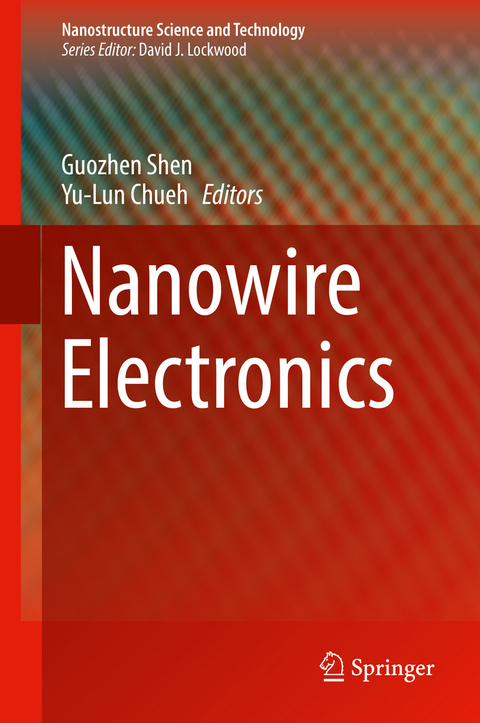
Nanowire Electronics (eBook)
VIII, 393 Seiten
Springer Singapore (Verlag)
978-981-13-2367-6 (ISBN)
This book gives a comprehensive overview of recent advances in developing nanowires for building various kinds of electronic devices. Specifically the applications of nanowires in detectors, sensors, circuits, energy storage and conversion, etc., are reviewed in detail by the experts in this field. Growth methods of different kinds of nanowires are also covered when discussing the electronic applications. Through discussing these cutting edge researches, the future directions of nanowire electronics are identified.
Dr. Guozhen Shen received his Ph.D. degree in Chemistry from University of Science and Technology of China in 2003. He then worked at Hanyang University, Korea(2004),National Institute for Materials Science, Japan(2005-2007) and University of Southern California (2009-2013). He was a professor at the Huazhong University of Science andTechnology (HUST)and the director of Energy Photonics Division and the assistant director of Wuhan National Laboratory for Optoelectronics (WNLO).In 2013, he joined Institute of Semiconductors, Chinese Academy of Sciences as a professor. He is the author or co-author of more than 200 research articles in peer reviewed journals and 9 book chapters, he also the editor of a book. His most recent research interests include the synthesis and characterization of one-dimensional nanostructures and their device applicationsin electronics and optoelectronics. Dr. Guozhen Shen is the assistant editor of Nanoscale Research Letters, the Asian Associate Editor of Journal of Nanoengineering and Nanomanufacturing, the Associate Editor of Reviews in Advanced Science and Engineering, and servers as the Editorial Board Member for more than 10 international journals.He was honored with the Distinguished Professor of the Hundred Talents Recruitment Program of Global Experts of Hubei in 2010, and the New Century Excellent Talents of Ministry of Education in 2011.
Dr. Yu-Lun Chueh received his Ph.D.from the Department of Materials Science and Engineering, National Tsing Hua University, Taiwan in 2006 and worked as a postdoctoral fellow in the Department of Electrical Engineering and Computer Sciences, with a joint appointment with Lawrence Berkeley National Laboratory from 2007 to 2009. He joined the
This book gives a comprehensive overview of recent advances in developing nanowires for building various kinds of electronic devices. Specifically the applications of nanowires in detectors, sensors, circuits, energy storage and conversion, etc., are reviewed in detail by the experts in this field. Growth methods of different kinds of nanowires are also covered when discussing the electronic applications. Through discussing these cutting edge researches, the future directions of nanowire electronics are identified.
Dr. Guozhen Shen received his Ph.D. degree in Chemistry from University of Science and Technology of China in 2003. He then worked at Hanyang University, Korea(2004),National Institute for Materials Science, Japan(2005–2007) and University of Southern California (2009-2013). He was a professor at the Huazhong University of Science andTechnology (HUST)and the director of Energy Photonics Division and the assistant director of Wuhan National Laboratory for Optoelectronics (WNLO).In 2013, he joined Institute of Semiconductors, Chinese Academy of Sciences as a professor. He is the author or co-author of more than 200 research articles in peer reviewed journals and 9 book chapters, he also the editor of a book. His most recent research interests include the synthesis and characterization of one-dimensional nanostructures and their device applicationsin electronics and optoelectronics. Dr. Guozhen Shen is the assistant editor of Nanoscale Research Letters, the Asian Associate Editor of Journal of Nanoengineering and Nanomanufacturing, the Associate Editor of Reviews in Advanced Science and Engineering, and servers as the Editorial Board Member for more than 10 international journals.He was honored with the Distinguished Professor of the Hundred Talents Recruitment Program of Global Experts of Hubei in 2010, and the New Century Excellent Talents of Ministry of Education in 2011. Dr. Yu-Lun Chueh received his Ph.D.from the Department of Materials Science and Engineering, National Tsing Hua University, Taiwan in 2006 and worked as a postdoctoral fellow in the Department of Electrical Engineering and Computer Sciences, with a joint appointment with Lawrence Berkeley National Laboratory from 2007 to 2009. He joined the
Preface 6
Contents 7
Chapter 1: X-Ray Spectroscopic Analysis of Electronic Properties of One-Dimensional Nanostructured Materials 9
1.1 Introduction 9
1.2 Synchrotron X-Ray Spectroscopies 14
1.3 Nanostructured Titania Arrays 16
1.3.1 Freestanding TiO2 Nanotube Array 16
1.3.2 QD Co-sensitized TiO2 Nanorod Arrays 22
1.4 Nanoflaky MnO2/Functionalized Carbon Nanotubes (CNT) 25
1.5 Conclusion and Future Perspective 34
References 34
Chapter 2: A Correlated Study of Nanotube/Nanowire Transistor Between TEM Inspection and Electrical Characterization 38
2.1 Introduction 38
2.2 Experimental Method 39
2.2.1 Multi-probe Stations 39
2.2.2 In Situ Nano-manipulation 41
2.3 Fabrication of Through-Hole Chip and Membrane Chip 42
2.4 Demonstration of the Correlated Study 45
2.4.1 Effects of Oxygen Bonding on Defective Semiconducting and Metallic Single-Walled Carbon Nanotube Bundles 45
2.4.2 Stacking Fault Induced Tunnel Barrier in Platelet Graphite Nanofiber 47
2.4.3 Self-Aligned Graphene Oxide Nanoribbon Stack with Gradient Bandgap for Visible-Light Photodetection 51
2.5 Conclusion 56
References 57
Chapter 3: Properties Engineering of III-V Nanowires for Electronic Application 59
3.1 Introduction 59
3.1.1 Synthesis of Nanowires 60
3.1.1.1 Bottom-Up Approach 60
3.1.1.2 Top-Down Approach 60
3.1.2 Applications of Nanowire Field-Effect Transistor 61
3.1.2.1 Integrated Circuit 61
3.1.2.2 Photodetector 61
3.1.2.3 Biosensor 61
3.1.3 NWFET Structure 62
3.1.3.1 Vertical Nanowire FET 62
3.1.3.2 Horizontal Nanowire FET 62
3.1.4 Advantages of III-V Compound Semiconductor NWs 63
3.1.5 Requirement on Properties Engineering 63
3.2 Surface Modification 64
3.2.1 Molecular Passivation 65
3.2.2 Metal Cluster Decoration 67
3.2.3 Surface Coating 69
3.2.3.1 By Thin Dielectric Layer 69
3.2.3.2 Core-Shell Nanowire 70
3.3 Contact Engineering 71
3.3.1 Contact Treatment 73
3.3.2 Nickelide Formation 74
3.3.3 Catalytic Tip Contact 75
3.4 Crystal Engineering 76
3.4.1 Catalyst Diameter Control 77
3.4.2 Growth Temperature 78
3.4.3 Source Flow Control 80
3.4.4 Challenges 80
3.5 Conclusions 81
References 82
Chapter 4: Probing Material Interfaces in Nanowire Devices Using Capacitive Measurements 89
4.1 Introduction 89
4.2 Diffused Junction of a Semiconductor Nanowire 90
4.2.1 Design of Test Structure and Measurement Scheme 91
4.2.2 Device Fabrication 91
4.2.3 Capacitance Measurement and Determination of Dopant Density 93
4.2.4 Dopant Profile 94
4.2.5 Summary 96
4.3 Surface States of Semiconductor Nanowires Characterized by Capacitance-Voltage Measurements 96
4.3.1 The Interface State Density of a Si Nanowire with Al2O3 Oxide 97
4.3.2 The Native Oxide in InAs nanowires 98
4.3.3 Capacitance for Mobility Determination 101
4.3.4 Summary and Future Work 102
4.4 Capacitance Measurement of Metal-Semiconductor Carbon Nanotube Contacts 104
4.4.1 Test Structure for C-V Measurement and Its Fabrication 104
4.4.2 Simulation of the C-V Measurements 105
4.4.3 Measurement Results 110
4.4.4 The Geometry of Metal-CNT Contacts 111
4.5 Summary and Future Work 114
References 114
Chapter 5: Metal-Semiconductor Compound Contacts to Nanowire Transistors 117
5.1 Introduction 117
5.2 Phases of Metal-Semiconductor Compound Contacts 118
5.2.1 Metal Silicide in Si NWs 118
5.2.2 Metal-Germanide in Ge NWs 123
5.2.3 Metal and III-V Compound Contacts 127
5.3 Kinetics of the Solid-State Reaction Between Metal and Semiconductor NWs 131
5.3.1 Kinetics Modeling: A Case Study of Ni-InGaAs Reaction 133
5.3.2 Atomic-Scale Dynamics 139
5.3.3 Modified Kinetic Process 140
5.4 Electrical Properties 145
5.4.1 Electrical Applications of Compound Contacts 145
5.4.2 Band Alignment and Charge Injection 150
5.4.3 Ultrashort Channel Devices 154
5.5 Conclusions 158
References 159
Chapter 6: Nanowire-Based Transparent Conductive Electrodes 165
6.1 Introduction 165
6.2 Synthesis, Fabrication, and Physical Properties of Transparent Conductive Oxides 166
6.2.1 N-Type Transparent Conductive Electrodes 168
6.2.1.1 Indium Tin Oxide Nanowires 168
6.2.1.2 Doped Zinc Oxide Nanowires 171
6.2.2 P-Type TCO Nanowires 177
6.3 Synthesis, Fabrication, and Physical Properties of Carbon Nanotube Networks 178
6.3.1 Transparent Conducting Carbon Nanotube Network Films 178
6.3.2 Nanomaterial Hybridized Transparent Conducting Nanotube Network Films 180
6.4 Synthesis, Fabrication, and Physical Properties of Metallic Nanowire Networks (MNW) 181
6.4.1 Silver Nanowires 181
6.4.2 Copper Nanowires 187
6.5 Applications 189
6.5.1 Photovoltaics 189
6.5.2 Light-Emitting Devices 192
6.5.3 Smart Windows and Displays 194
6.5.4 Transparent Film Heaters 195
6.5.5 Other Applications 197
6.6 Summary 197
References 201
Chapter 7: One-Dimensional Nanowire-Based Heterostructures for Gas Sensors 207
7.1 Introduction 207
7.2 Advantages of Nanowires for Application in Gas Sensing 209
7.3 Nanowire-Nanoparticle Heterostructures and Gas Sensing Mechanism 211
7.3.1 Metal Oxide-Metal Heteronanowires 214
7.3.2 Metal Oxide-Metal Oxide Heteronanowires 220
7.3.2.1 P-N Heteronanowires 220
7.3.2.2 N-N Heteronanowire 222
7.4 Gas Sensing Performances of Heteronanowires 224
7.4.1 Enhanced Sensing Performance of Metal/Metal Oxide Heteronanowires 225
7.4.2 Enhanced Sensing Performance of P-N Heteronanowires 230
7.4.3 Enhanced Sensing Performance of N-N Heteronanowires 232
7.5 Summary 234
References 235
Chapter 8: Silicon Carbide Nanowires and Electronics 242
8.1 Introduction 242
8.2 Synthesis and Design of SiC Nanowires 243
8.2.1 SiC Nanowires Growth in Vapor 244
8.2.1.1 VLS Growth 246
8.2.1.2 VS Growth 248
8.2.2 SiC Nanowires Growth in Liquid 249
8.2.2.1 Solvothermal Method 249
8.2.2.2 Electrochemical Etching 251
8.2.3 Doping of SiC Nanowires 251
8.2.3.1 p-Type Doping 252
8.2.3.2 n-Type Doping 252
8.2.4 SiC Nanowires with Complex Morphologies 254
8.2.4.1 Hierarchical SiC Nanowires 254
8.2.4.2 Beaded SiC Nanochains 257
8.2.4.3 Bamboo-Like SiC Nanowires 259
8.2.4.4 Twinned SiC Nanowires 259
8.2.4.5 Bicrystalline SiC Nanowires 261
8.2.5 Coaxial Core-Shell SiC Nanowires 264
8.2.5.1 SiC-Core-Based Core-Shell Nanowires 264
8.2.5.2 SiC-Shell-Based Core-Shell Nanowires 269
8.2.6 Aligned SiC Nanowire Arrays 271
8.2.6.1 Homoepitaxial Growth 272
8.2.6.2 Electrochemical Etching 273
8.2.6.3 Converted from Si Nanowire Arrays by the In Situ Carbonizing Route 276
8.2.6.4 Template-Assisted Synthesis 277
8.3 Electronic Applications of SiC Nanowires 277
8.3.1 Field Emission Applications 278
8.3.1.1 Field Emission Phenomena 278
8.3.1.2 Enhanced FE Properties by Growing SiC Nanowires with Sharp Tips 281
8.3.1.3 Enhanced FE Properties by Doped SiC Nanowires 283
8.3.1.4 Enhanced FE Properties by Surface-Decorated SiC Nanowire Emitters with Nanoparticles 287
8.3.1.5 Enhanced FE Properties by Orientation-Ordered SiC Nanowire Arrays 291
8.3.1.6 Enhanced FE Properties of SiC Nanowires with Other Morphologies 295
8.3.1.7 FE Properties of Flexible SiC Nanowire Cathodes 297
8.3.2 Supercapacitors 303
8.3.2.1 Supercapacitors with SiC Nanowire Electrodes 304
8.3.2.2 Supercapacitors with SiC Nanowire Composite Electrodes 305
8.3.3 Photocatalysts 309
8.3.3.1 Photocatalytic Degradation of Pollutants 309
8.3.3.2 Photocatalytic Hydrogen Production 310
8.3.3.3 Photocatalytic CO2 Conversion 312
8.3.4 Field-Effect Transistors 312
8.3.4.1 Electrical Properties of SiC Nanowire-Based FETs 313
8.3.4.2 Improvement of Source/Drain Ohmic Contact by Ni-Based Contacts 314
8.3.5 Pressure Sensors 317
8.3.5.1 Piezoresistive Effect in Semiconductors 318
8.3.5.2 The Piezoresistive Effect in SiC Nanowires 319
8.4 Conclusions and Outlooks 323
References 324
Chapter 9: Nanowire Bioelectronics 341
9.1 Nanowire Bioelectronics for the Detection of Biological Molecules 343
9.2 Nanowire Bioelectronics for Extracellular Recording 347
9.3 Nanowire Bioelectronics for Intracellular Recording 349
9.4 Nanowires for 3D Interfacing with Biological Systems 352
9.5 Conclusion and Prospects 353
References 354
Chapter 10: Nanowires for Triboelectric Nanogenerators 357
10.1 Introduction of Triboelectric Nanogenerators 357
10.2 Nanowire-Based Flexible TENGs 360
10.3 Nanowire-Based Self-Powered Electronic Skins 365
10.4 Summary 365
References 367
Chapter 11: Nanowire-Based Lasers 370
11.1 Introduction 370
11.2 Nanowire Lasing Mechanisms 371
11.2.1 Waveguiding Mechanism 372
11.2.2 Gain and Losses 375
11.3 Materials for Nanowire Lasers 381
11.4 Wavelength Tunability in Nanowire Lasers 382
11.5 New Nanowire Laser Cavity Structures 386
11.6 Surface Plasmon Polariton Lasers 388
11.7 Electrical Excitation of Nanowire Lasers 390
References 392
| Erscheint lt. Verlag | 23.11.2018 |
|---|---|
| Reihe/Serie | Nanostructure Science and Technology |
| Zusatzinfo | VIII, 393 p. 222 illus. |
| Verlagsort | Singapore |
| Sprache | englisch |
| Themenwelt | Technik ► Elektrotechnik / Energietechnik |
| Technik ► Maschinenbau | |
| Schlagworte | Energy Conversion and Storage • Field emitter • Flexible electronics • Integrated Circuits • Metal Oxide Nanowires • microelectronics • Semiconductor Nanostructures |
| ISBN-10 | 981-13-2367-4 / 9811323674 |
| ISBN-13 | 978-981-13-2367-6 / 9789811323676 |
| Haben Sie eine Frage zum Produkt? |
Größe: 17,9 MB
DRM: Digitales Wasserzeichen
Dieses eBook enthält ein digitales Wasserzeichen und ist damit für Sie personalisiert. Bei einer missbräuchlichen Weitergabe des eBooks an Dritte ist eine Rückverfolgung an die Quelle möglich.
Dateiformat: PDF (Portable Document Format)
Mit einem festen Seitenlayout eignet sich die PDF besonders für Fachbücher mit Spalten, Tabellen und Abbildungen. Eine PDF kann auf fast allen Geräten angezeigt werden, ist aber für kleine Displays (Smartphone, eReader) nur eingeschränkt geeignet.
Systemvoraussetzungen:
PC/Mac: Mit einem PC oder Mac können Sie dieses eBook lesen. Sie benötigen dafür einen PDF-Viewer - z.B. den Adobe Reader oder Adobe Digital Editions.
eReader: Dieses eBook kann mit (fast) allen eBook-Readern gelesen werden. Mit dem amazon-Kindle ist es aber nicht kompatibel.
Smartphone/Tablet: Egal ob Apple oder Android, dieses eBook können Sie lesen. Sie benötigen dafür einen PDF-Viewer - z.B. die kostenlose Adobe Digital Editions-App.
Zusätzliches Feature: Online Lesen
Dieses eBook können Sie zusätzlich zum Download auch online im Webbrowser lesen.
Buying eBooks from abroad
For tax law reasons we can sell eBooks just within Germany and Switzerland. Regrettably we cannot fulfill eBook-orders from other countries.
aus dem Bereich


