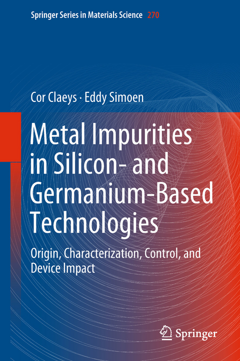
Metal Impurities in Silicon- and Germanium-Based Technologies (eBook)
XXXIII, 464 Seiten
Springer-Verlag
978-3-319-93925-4 (ISBN)
Cor Claeys is a Professor at the KU Leuven (Belgium) since 1990. He was at imec, Leuven, Belgium from 1984 till 2016. His main interests are silicon technology, device physics, low-frequency noise phenomena, radiation effects, defect engineering and material characterization. He has co-edited a book on “Low Temperature Electronics” and “Germanium-Based Technologies: From Materials to Devices” and co-authored monographs on “Radiation Effects in Advanced Semiconductor Materials and Devices,” “Fundamental and Technological Aspects of Extended Defects in Germanium” and “Random Telegraph Signals in Semiconductor Devices.” He (co)authored 15 book chapters, over 1100 conference presentations and more than 1300 technical papers. He is editor/co-editor of 60 Conference Proceedings. Prof. Claeys is a Fellow of the Electrochemical Society and of the IEEE. He was Founder of the IEEE Electron Devices Benelux Chapter, Chair of the IEEE Benelux Section, elected Board of Governors Member of the Electron Devices Society and the EDS Vice President for Chapters and Regions. He was EDS President in 2008-2009 and Division Director on the IEEE Board of Directors in 2012-2013. He is a recipient of the IEEE Third Millennium Medal and received the IEEE EDS Distinguished Service Award.Within the Electrochemical Society, he was the Chair of the Electronics & Photonics Division from 2001 to 2003. In 2004, he received the Electronics and Photonics Division Award. In 2016 he received the Semi China Special Recognition Award for outstanding involvement in the China Semiconductor Technology International Conference (CSTIC). Eddy Simoen obtained his Bachelor’s (1976–1978) and Master’s degrees in Physics Engineering (1978–1980), as well as his Ph.D. in Engineering (1985), from Ghent University (Belgium). He is currently a Specialist at imec (Leuven, Belgium), involved in the study of defect and strain engineering in high-mobility and epitaxial substrates and defect studies in germanium and III–V compounds (AlN; GaN, InP, etc). Another current focus point is the study of 1-transistor memories based on bulk FinFET and Ultra-thin Buried Oxide (UTBOX) Silicon-on-Insulator (SOI), using low-frequency noise. In 2013, he was appointed a part-time Professor at Ghent University. He is a member of the IEEE and ECS and became an ECS Fellow in 2016. In these fields, he has (co-) authored over 1500 Journal and Conference papers, 12 book chapters and a monograph on Radiation Effects in Advanced Semiconductor Devices and Materials (Springer, 2002). He was also a co-editor of the book on Germanium-based Technologies – from Materials to Devices (Elsevier March 2007; Chinese translation 2010). Another book on the “Fundamental and Technological Aspects of Extended Defects in Germanium” was published by Springer in January 2009. In 2016 he published “Random Telegraph Signals in Semiconductor Devices” with IOP. He is also a co-inventor of two patents.
Preface 7
Contents 9
Abbreviations 14
Symbols 21
Greek Symbols 29
1 Introduction 32
References 38
2 Basic Properties of Transition Metals in Semiconductors 39
2.1 Solid Solubility 40
2.2 Diffusivity 43
2.2.1 Ion Pairing and Doping Effects 46
2.3 Segregation and Precipitation 50
2.4 Electrical Properties of Transition Metals 56
References 62
3 Source of Metals in Si and Ge Crystal Growth and Processing 66
3.1 Crystal Growth 67
3.2 Wet Wafer Cleaning Processes 70
3.2.1 Contamination in Si Cleaning Technology 70
3.2.2 Contamination in Ge Cleaning Technology 75
3.3 Dry Vapor Phase Wafer Cleaning 76
3.4 Photoresist Deposition and Stripping 76
3.5 Wafer Handling 79
3.6 Ion Implantation 80
3.7 Thermal Processing 84
3.8 Metal Layers in Device Fabrication 87
3.8.1 Silicidation and Germanidation 88
3.8.2 Metallization 91
3.8.3 3D Integration—Through Silicon Vias (TSV) 92
3.8.4 Ferroelectric Memories 94
References 96
4 Characterization and Detection of Metals in Silicon and Germanium 104
4.1 Chemical Analysis of Metals 105
4.1.1 Elemental Analysis of Surface Metal Contamination 106
4.1.2 Elemental Analysis of Bulk Metal Contamination 108
4.1.3 Electron Paramagnetic Resonance 111
4.1.4 Mössbauer Spectroscopy 114
4.2 Structural Analysis 115
4.2.1 Structural Analysis of Metal Precipitates 116
4.2.2 Structural Analysis of Metal-Related Point Defects 118
4.3 Electrical Analysis 118
4.3.1 Theoretical and Practical Considerations for Lifetime Measurements 120
4.3.2 Surface Photo Voltage Lifetime Analysis 124
4.3.3 PhotoConductance Decay (PCD) and QSS-PC Method 127
4.3.4 ELYMAT 129
4.3.5 PL Imaging 131
4.3.6 Carrier Lifetime by IR Imaging 133
4.3.7 Lifetime Mapping of Extended Defects 134
4.3.8 MOS Generation Lifetime Techniques 137
4.3.9 Deep-Level Transient Spectroscopy 139
4.4 Strategy for Metal Contamination Monitoring 143
References 145
5 Electrical Activity of Iron and Copper in Si, SiGe and Ge 153
5.1 Iron 154
5.1.1 Configurations of Fe 154
5.1.1.1 Interstitial and Substitutional Fe 154
5.1.1.2 Dopant-Iron Pairs 156
5.1.1.3 Small Fe-Related Clusters and Fe-Related Complexes 159
5.1.1.4 Fe Precipitation 160
5.1.2 Electrical Properties of Fe 164
5.1.2.1 Fei and FeA Pairs in Silicon 164
5.1.2.2 Fe-Related Point Defects in Si and Ge 170
5.1.2.3 Fe-Related Clusters and Precipitates 173
5.1.2.4 Fe Activation of Extended Defects 174
5.1.3 Detection and Identification of Fe in Silicon 175
5.2 Copper 179
5.2.1 Configurations of Copper 180
5.2.1.1 Cu-Related Point Defects 180
5.2.1.2 Heterogeneous Precipitation of Copper 181
5.2.1.3 Homogeneous Precipitation of Copper 186
5.2.1.4 Precipitation Versus Out-Diffusion 188
5.2.2 Electrical Activity of Cu 191
5.2.2.1 Copper-Related Point Defects 191
5.2.2.2 Electrical Activity of Precipitated Copper 195
5.2.2.3 Copper Activation and Passivation of Extended Defects 198
5.2.3 Detection of Copper 200
5.2.3.1 Lifetime-Based Sensitive Copper Detection 200
5.2.3.2 Transient Ion Drift Analysis of Copper in Silicon 208
References 210
6 Electrical Properties of Metals in Si and Ge 225
6.1 Nickel in Si and Ge 226
6.1.1 Ni-related Point Defects and Complexes 226
6.1.2 Precipitation and Co-precipitation of Ni 227
6.1.2.1 Homogeneous and Heterogeneous Precipitation of NiSi2 227
6.1.2.2 Co-precipitation of Nickel in Silicon 230
6.1.3 Electrical and Optical Activity of Ni 232
6.1.3.1 Nickel-Related Point Defects and Complexes 232
6.1.3.2 Electrically Active Point Defects in Ge and SiGe 234
6.1.3.3 Electrical Activity of Nickel Precipitates 235
6.1.3.4 Nickel-Decorated Extended Defects 239
6.1.4 Impact of Ni on Recombination Lifetime 240
6.2 Cobalt in Si and Ge 243
6.2.1 Co-related Species in Si 243
6.2.1.1 Atomic and Clustered Species 243
6.2.1.2 Buried CoSi2 Formation 244
6.2.2 Electrical and Optical Activity of Co in Si 245
6.2.2.1 Levels from Resistivity and Photoconductivity 246
6.2.2.2 Deep Levels from Space-Charge Transient Techniques (DLTS) 246
6.2.3 Impact on Lifetime 251
6.3 Chromium in Si and Ge 254
6.3.1 Configurations of Cr in Si 254
6.3.2 Electrical and Optical Activity of Cr in Si 254
6.3.2.1 Electrical Properties 254
6.3.2.2 Optical Properties 257
6.3.2.3 Impact of Cr on Lifetime in Silicon 258
6.3.2.4 Identification of Cr in Silicon by Lifetime Measurements 261
6.4 Titanium 262
6.5 Molybdenum 264
6.6 Palladium 267
6.7 Platinum 269
6.8 Gold 271
6.9 Scandium 274
6.10 Vanadium 274
6.11 Manganese 276
6.12 Zinc 278
6.13 Zirconium 280
6.14 Niobium 280
6.15 Ruthenium 281
6.16 Rhodium 283
6.17 Silver 285
6.18 Cadmium 287
6.19 Hafnium 287
6.20 Tantalum 289
6.21 Tungsten 289
6.22 Rhenium–Osmium 290
6.23 Iridium 292
6.24 Mercury 294
References 294
7 Impact of Metals on Silicon Devices and Circuits 314
7.1 MOS Capacitors 315
7.1.1 Impact of Metal Contamination on MOS Capacitors 316
7.1.1.1 Diffusion, Precipitation and Segregation of Metals in Dielectric Layers 316
7.1.1.2 Impact of Fe on MOS Capacitors 319
7.1.1.3 Impact of Nickel on MOS Capacitors 320
7.1.2 Impact of Copper on MOS Capacitors 321
7.1.2.1 Basic Properties of Copper in SiO2 321
7.1.2.2 Diffusion of Cu in Low-? Dielectrics 323
7.1.2.3 Impact of Cu on MOS Capacitors 325
7.1.2.4 Impact on Interlayer Dielectric Integrity 331
7.2 Impact on p-n Junction Devices and Schottky Barriers 333
7.2.1 Metal Contamination in p-n Junctions 333
7.2.1.1 Impact of Copper 333
7.2.1.2 Impact of Other TMs 336
7.2.2 Silicidation-Induced Metal Contamination 337
7.2.2.1 Ti-Silicidation 337
7.2.2.2 Co-silicidation 338
7.2.2.3 Ni-Silicidation 342
7.2.3 Metal Contamination in Silicon Solar Cells 348
7.2.3.1 Impact Defects on Solar Cell Parameters 349
7.2.3.2 Impact Specific TMs on Solar Cells 351
7.2.3.3 Acceptable Metal Levels in Mc-Si Solar Cells 354
7.2.4 Impact on Schottky Barriers 355
7.3 Impact on Transistors and on Circuit Operation and Yield 358
7.3.1 Impact on Transistors 358
7.3.2 Impact on Circuits 359
7.3.3 Impact on Yield 363
References 363
8 Gettering and Passivation of Metals in Silicon and Germanium 378
8.1 Gettering Strategies 379
8.1.1 Metal Gettering Mechanisms 381
8.2 Backside Gettering Mechanisms 383
8.2.1 Glass Layer Gettering 383
8.2.2 Thin Layer Gettering 386
8.2.2.1 Aluminum Films 386
8.2.2.2 Silicon Nitride and Polysilicon Layers 387
8.2.3 Ion Implantation Gettering 389
8.3 Intrinsic Gettering Mechanisms 390
8.4 Frontside Gettering Techniques 396
8.4.1 Buried Epitaxial or Porous Si Layer 396
8.4.2 Ion Implantation 397
8.4.2.1 Nano Cavities 399
8.4.2.2 Near-Surface Proximity Gettering 401
8.5 Gettering in SOI Material 403
8.5.1 SIMOX SOI Material 403
8.5.2 Ultra-thin Body and BOX (UTBB) 405
8.6 Gettering Processes for Photovoltaics 405
8.7 Modeling Gettering Processes 406
References 407
9 Modeling of Metal Properties in Si, Si1?xGex and Ge 416
9.1 Modeling Approaches 417
9.1.1 EPR-Based Models 417
9.1.2 First-Principles Calculations 418
9.1.3 Calculation of Parameters in DFT 421
9.2 Configurations of Individual Metal Atoms 423
9.2.1 Trends in the Properties of 3d TMs in Si and Ge 423
9.2.2 Iron in Si and SiGe 429
9.2.3 Copper in Si 430
9.2.4 Cobalt in Si 431
9.2.5 Vanadium in Si 432
9.2.6 Manganese in Si and Ge 432
9.3 Diffusion of Metal Atoms in Si and Ge 434
9.3.1 Elastic Energy Approach 434
9.3.2 Thermodynamic Approach 436
9.3.3 DFT and MD Calculations 436
9.4 Interactions of Metals with Dopants, H, O, C in Si and Ge 439
9.4.1 Interaction with Dopants 439
9.4.2 Interaction with Hydrogen 443
9.4.3 Interaction with Oxygen and Carbon 446
9.5 Interactions of Metals with Other Defects, Clustering and Gettering 447
9.5.1 Metal Pairs, Clusters and Precipitates 447
9.5.2 Interaction with Implantation and Extended Defects 450
9.5.3 First-Principles Studies of Metal Gettering 452
References 455
Index 461
| Erscheint lt. Verlag | 13.8.2018 |
|---|---|
| Reihe/Serie | Springer Series in Materials Science |
| Zusatzinfo | XXXIII, 438 p. 215 illus., 207 illus. in color. |
| Verlagsort | Cham |
| Sprache | englisch |
| Themenwelt | Technik ► Elektrotechnik / Energietechnik |
| Technik ► Maschinenbau | |
| Schlagworte | Defect Engineering • Defects and Device Performance • Device Yield Improvement • Metal Gettering • Metal Precipitation and Segregation • Semiconductor Device Fabrication |
| ISBN-10 | 3-319-93925-4 / 3319939254 |
| ISBN-13 | 978-3-319-93925-4 / 9783319939254 |
| Haben Sie eine Frage zum Produkt? |
Größe: 14,5 MB
DRM: Digitales Wasserzeichen
Dieses eBook enthält ein digitales Wasserzeichen und ist damit für Sie personalisiert. Bei einer missbräuchlichen Weitergabe des eBooks an Dritte ist eine Rückverfolgung an die Quelle möglich.
Dateiformat: PDF (Portable Document Format)
Mit einem festen Seitenlayout eignet sich die PDF besonders für Fachbücher mit Spalten, Tabellen und Abbildungen. Eine PDF kann auf fast allen Geräten angezeigt werden, ist aber für kleine Displays (Smartphone, eReader) nur eingeschränkt geeignet.
Systemvoraussetzungen:
PC/Mac: Mit einem PC oder Mac können Sie dieses eBook lesen. Sie benötigen dafür einen PDF-Viewer - z.B. den Adobe Reader oder Adobe Digital Editions.
eReader: Dieses eBook kann mit (fast) allen eBook-Readern gelesen werden. Mit dem amazon-Kindle ist es aber nicht kompatibel.
Smartphone/Tablet: Egal ob Apple oder Android, dieses eBook können Sie lesen. Sie benötigen dafür einen PDF-Viewer - z.B. die kostenlose Adobe Digital Editions-App.
Zusätzliches Feature: Online Lesen
Dieses eBook können Sie zusätzlich zum Download auch online im Webbrowser lesen.
Buying eBooks from abroad
For tax law reasons we can sell eBooks just within Germany and Switzerland. Regrettably we cannot fulfill eBook-orders from other countries.
aus dem Bereich
