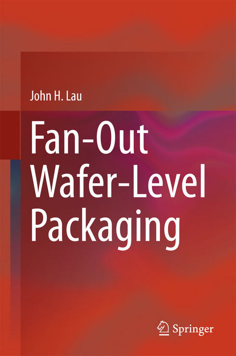
Fan-Out Wafer-Level Packaging (eBook)
XX, 303 Seiten
Springer Singapore (Verlag)
978-981-10-8884-1 (ISBN)
This comprehensive guide to fan-out wafer-level packaging (FOWLP) technology compares FOWLP with flip chip and fan-in wafer-level packaging. It presents the current knowledge on these key enabling technologies for FOWLP, and discusses several packaging technologies for future trends. The Taiwan Semiconductor Manufacturing Company (TSMC) employed their InFO (integrated fan-out) technology in A10, the application processor for Apple's iPhone, in 2016, generating great excitement about FOWLP technology throughout the semiconductor packaging community. For many practicing engineers and managers, as well as scientists and researchers, essential details of FOWLP - such as the temporary bonding and de-bonding of the carrier on a reconstituted wafer/panel, epoxy molding compound (EMC) dispensing, compression molding, Cu revealing, RDL fabrication, solder ball mounting, etc. - are not well understood.
Intended to help readers learn the basics of problem-solving methods and understand the trade-offs inherent in making system-level decisions quickly, this book serves as a valuable reference guide for all those faced with the challenging problems created by the ever-increasing interest in FOWLP, helps to remove roadblocks, and accelerates the design, materials, process, and manufacturing development of key enabling technologies for FOWLP.
SPECIALIZED PROFESSIONAL COMPETENCE
Design, analysis, materials, process, manufacturing, qualification, reliability, testing, and thermal management of electronic and optoelectronic components and systems. SMT, fan-out/fan-in WLP, TSV, 3D IC Integration, heterogeneous integration and SiP. Leadfree soldering, manufacturing, and solder joint reliability. Management of a R&D Laboratory and Company.
BACKGROUND AND PROFESSIONAL EXPERIENCE
Ph.D. (Theoretical and Applied Mechanics), University of Illinois, Urbana, IL (1977)
M.S. (Engineering Physics), University of Wisconsin, Madison, WI (1974)
M.S. (Structural Mechanics), University of British Columbia, Vancouver, BC (1973)
M.S. (Management Science), Fairleigh Dickinson University, Teaneck, NJ (1981)
B.S. (Civil Engineering), National Taiwan University, Taipei, Taiwan (1970)
ASM Pacific Technology (Sr. Technical Advisor), Hong Kong, July 2014 - Present
Industrial Technology Research Institute (ITRI Fellow), Taiwan, Jan 2010 - June 2014
Hong Kong University of Science & Technology (Visiting Professor), Jan 2009 - Jan 2010
Institute of Microelectronic, (Director, System Packaging Lab), Singapore, 2006 - Jan 2009
Agilent Technologies, Inc. (Sr. Interconnection Specialist), Santa Clara, CA, 2000-2006
Express Packaging Systems, Inc., (President), Palo Alto, CA, 1995-2000
Hewlett-Packard Labs/Company (Senior MTS/Individual Contributor), Palo Alto, CA, 1984-1995
Sandia National Laboratories (Member of Technical Staff), Albuquerque, NM, 1982-1983
Bechtel Power Corporation (Lead Engineer), San Francisco, CA, 1981-1982
Ebasco (Lead Engineer), New York, NY, 1978-1980
Exxon Production and Research Company (Research Engineer), Houston, TX, 1977-1978
Editorial Board of ASME Transactions, Journal of Electronic Packaging, 1989-1999
Editorial Board of IEEE Transactions on Components, Packaging, Manufacture Technology, 1990-1995
Editor-in-Chief, Circuit World, 1998-2000.
Program Chair ('90) to General Chair ('92) of the IEEE/CPMT IEMTS
Program Chair ('93) to General Chair ('95) of the IEEE/CPMT ECTC
Publication Chair for IEEE/ECTC
Symposium Organizer/Chair of the ASME Winter Annual Meeting, 1987-2002
ASME Distinguish Lecturer (2000-2003), IEEE/CPMT Distinguish Lecturer (1998-present)
ASME Worcester Reed Warner Medal (2015)
IEEE Components Packaging and Manufacturing Technology Field Award (2013)
IMAPS William Ashman Achievement Award (2013)Pan Wen Yuan Distinguished Research Award (2011)
IEEE/CPMT Outstanding Sustained Technical Contribution Award (2010)
Best IEEE Transactions Paper Award (2010 Components Packaging and Manufacturing Technology)
Outstanding Paper Award (2009 IEEE EPTC)
SME Total Excellence in Electronics Manufacturing Award (2001)
Best ASME Transactions Paper Award (2000 Journal of Electronic Packaging)
IEEE/CPMT Outstanding Contribution Awards (2000)
IEEE Meritorious Achievement Award in Continuing Education (2000)
ASME/EEP Technical Achievement Award (1998)
IEEE/CPMT Manufacturing Awards (1994)
Best of Conference Paper Award (1989 IEEE ECTC)
IEEE Fellow (since 1994), ASME Fellow (since 1999), IMAPS Fellow (since 2013)
Over 20 books, 450 peer-reviewed papers, 30 issued and pending patents, and 290 keynotes/lectures.
This comprehensive guide to fan-out wafer-level packaging (FOWLP) technology compares FOWLP with flip chip and fan-in wafer-level packaging. It presents the current knowledge on these key enabling technologies for FOWLP, and discusses several packaging technologies for future trends. The Taiwan Semiconductor Manufacturing Company (TSMC) employed their InFO (integrated fan-out) technology in A10, the application processor for Apple's iPhone, in 2016, generating great excitement about FOWLP technology throughout the semiconductor packaging community. For many practicing engineers and managers, as well as scientists and researchers, essential details of FOWLP - such as the temporary bonding and de-bonding of the carrier on a reconstituted wafer/panel, epoxy molding compound (EMC) dispensing, compression molding, Cu revealing, RDL fabrication, solder ball mounting, etc. - are not well understood. Intended to help readers learn the basics of problem-solving methods and understand the trade-offs inherent in making system-level decisions quickly, this book serves as a valuable reference guide for all those faced with the challenging problems created by the ever-increasing interest in FOWLP, helps to remove roadblocks, and accelerates the design, materials, process, and manufacturing development of key enabling technologies for FOWLP.
SPECIALIZED PROFESSIONAL COMPETENCEDesign, analysis, materials, process, manufacturing, qualification, reliability, testing, and thermal management of electronic and optoelectronic components and systems. SMT, fan-out/fan-in WLP, TSV, 3D IC Integration, heterogeneous integration and SiP. Leadfree soldering, manufacturing, and solder joint reliability. Management of a R&D Laboratory and Company. BACKGROUND AND PROFESSIONAL EXPERIENCE Ph.D. (Theoretical and Applied Mechanics), University of Illinois, Urbana, IL (1977) M.S. (Engineering Physics), University of Wisconsin, Madison, WI (1974) M.S. (Structural Mechanics), University of British Columbia, Vancouver, BC (1973) M.S. (Management Science), Fairleigh Dickinson University, Teaneck, NJ (1981) B.S. (Civil Engineering), National Taiwan University, Taipei, Taiwan (1970) ASM Pacific Technology (Sr. Technical Advisor), Hong Kong, July 2014 - Present Industrial Technology Research Institute (ITRI Fellow), Taiwan, Jan 2010 – June 2014 Hong Kong University of Science & Technology (Visiting Professor), Jan 2009 – Jan 2010 Institute of Microelectronic, (Director, System Packaging Lab), Singapore, 2006 - Jan 2009 Agilent Technologies, Inc. (Sr. Interconnection Specialist), Santa Clara, CA, 2000-2006 Express Packaging Systems, Inc., (President), Palo Alto, CA, 1995-2000 Hewlett-Packard Labs/Company (Senior MTS/Individual Contributor), Palo Alto, CA, 1984-1995 Sandia National Laboratories (Member of Technical Staff), Albuquerque, NM, 1982-1983 Bechtel Power Corporation (Lead Engineer), San Francisco, CA, 1981-1982 Ebasco (Lead Engineer), New York, NY, 1978-1980 Exxon Production and Research Company (Research Engineer), Houston, TX, 1977-1978 Editorial Board of ASME Transactions, Journal of Electronic Packaging, 1989-1999 Editorial Board of IEEE Transactions on Components, Packaging, Manufacture Technology, 1990-1995 Editor-in-Chief, Circuit World, 1998-2000. Program Chair ('90) to General Chair ('92) of the IEEE/CPMT IEMTS Program Chair ('93) to General Chair ('95) of the IEEE/CPMT ECTC Publication Chair for IEEE/ECTC Symposium Organizer/Chair of the ASME Winter Annual Meeting, 1987-2002 ASME Distinguish Lecturer (2000-2003), IEEE/CPMT Distinguish Lecturer (1998-present) ASME Worcester Reed Warner Medal (2015) IEEE Components Packaging and Manufacturing Technology Field Award (2013) IMAPS William Ashman Achievement Award (2013) Pan Wen Yuan Distinguished Research Award (2011) IEEE/CPMT Outstanding Sustained Technical Contribution Award (2010) Best IEEE Transactions Paper Award (2010 Components Packaging and Manufacturing Technology) Outstanding Paper Award (2009 IEEE EPTC) SME Total Excellence in Electronics Manufacturing Award (2001) Best ASME Transactions Paper Award (2000 Journal of Electronic Packaging) IEEE/CPMT Outstanding Contribution Awards (2000) IEEE Meritorious Achievement Award in Continuing Education (2000) ASME/EEP Technical Achievement Award (1998) IEEE/CPMT Manufacturing Awards (1994) Best of Conference Paper Award (1989 IEEE ECTC) IEEE Fellow (since 1994), ASME Fellow (since 1999), IMAPS Fellow (since 2013) Over 20 books, 450 peer-reviewed papers, 30 issued and pending patents, and 290 keynotes/lectures.
Preface 5
Acknowledgements 8
Contents 10
About the Author 18
1 Patent Issues of Fan-Out Wafer-Level Packaging 20
1.1 Introduction 20
1.2 Functions of Semiconductor Packaging 20
1.3 Level of Semiconductor Packaging 21
1.4 Patents Impacting the Semiconductor Packaging 21
1.4.1 Leadframe 22
1.4.2 Organic Substrate with Solder Balls 23
1.4.3 Fan-In Wafer-Level Packaging 24
1.4.4 Fan-Out Wafer-Level Packaging 26
1.5 Major Claims of Infineon’s Patent 29
1.6 TSMC InFO-WLP 31
1.7 Fraunhofer IZM FOPLP 34
1.8 Ball/Bump Pitch/Size of PBGA, fcPBGA, WLCSP, and FOWLP 34
1.9 Summary and Recommendations 36
References 37
2 Flip Chip Technology Versus FOWLP 40
2.1 Introduction 40
2.2 Wafer Bumping 43
2.2.1 C4 Bumps 43
2.2.2 C2 (Cu Pillar with Solder Cap) Bumps 44
2.3 Flip Chip Package Substrates 46
2.3.1 Surface Laminar Circuit (SLC) Technology 46
2.3.2 Integrated Thin-Film High-Density Organic Package (i-THOP) 47
2.3.3 Coreless Substrate 49
2.3.4 Bump-on-Lead (BOL) 50
2.3.5 Embedded Trace Substrate (ETS) 51
2.4 Flip Chip Assembly 53
2.4.1 Cu-to-Cu TCB Direct Bonding 53
2.4.2 C4 Solder Mass Reflow 54
2.4.3 C2 Solder Mass Reflow 55
2.4.4 C2 TCB 55
2.4.4.1 C2 TCB with Low Bonding Force 56
2.4.4.2 C2 TCB with High Bonding Force 56
2.5 Underfill/Reliability 56
2.6 Post-assembly Underfill 57
2.6.1 Capillary Underfill (CUF) 57
2.6.2 Molded Underfill (MUF) 57
2.6.3 Printed Underfill 58
2.6.3.1 A New Stencil Design 59
2.6.3.2 Test Chip 60
2.6.3.3 Test Substrates 61
2.6.3.4 Flip Chip Assemblies 63
2.6.3.5 Stencil Designs 65
2.6.3.6 Test Matrix 65
2.6.3.7 Baking Substrates 66
2.6.3.8 Printing Process 67
2.6.3.9 Capillary Action and Curing 67
2.6.3.10 Effects of Underfill Viscosity, Thermal Enhancement, and Multiple Prints 67
2.6.3.11 Cross Sections 69
2.6.3.12 Underfill Filler Density 70
2.6.3.13 Shearing Test 70
2.7 Preassembly Underfill 71
2.8 Cu–Cu Direct Hybrid Bonding 75
2.9 Flip Chip Technology Versus FOWLP 76
2.10 Summary and Recommendations 77
References 79
3 Fan-in Wafer-Level Packaging Versus FOWLP 88
3.1 Introduction 88
3.2 Fan-in Wafer-Level Packaging (WLP) 89
3.3 Wafer-Level Chip Scale Packages (WLCSPs) 89
3.4 WLCSP Test Vehicle 90
3.4.1 The Chip 90
3.4.2 The WLCSP 90
3.4.3 WLCSP Key Process Steps 91
3.5 PCB Assembly of the WLCSP 92
3.6 Thermal Cycling Test of WLCSP-PCB Assembly 95
3.6.1 Thermal Cycling Condition 95
3.6.2 Crack Length Distribution of All Solder Joints 95
3.6.3 Crack Propagation of the Corner Solder Joint 96
3.6.4 Fatigue Crack Growth Rate 97
3.7 Fracture Characteristics of the Corner Solder Joint—Solder Material and Properties 100
3.8 Fracture Characteristics of the Corner Solder Joint—Geometry 102
3.9 Fracture Characteristics of the Corner Solder Joint—Elastic Thermal Fatigue Life Prediction Model (?K) 103
3.9.1 Boundary Value Problem 103
3.9.2 Thermal Fatigue Life Prediction Model 105
3.9.3 Summary and Recommendations 107
3.10 Fracture Characteristics of the Corner Solder Joint—Plastic Thermal Fatigue Life Prediction Model (?J) 108
3.10.1 Boundary Condition and Results 109
3.10.2 Thermal Fatigue Life Prediction Model 109
3.10.3 Summary and Recommendations 113
3.11 Fracture Characteristics of the Corner Solder Joint—Creep Thermal Fatigue Life Prediction Model (?W) 114
3.11.1 Assumptions 114
3.11.2 Boundary Conditions 114
3.11.3 Deformed Shape, Stress, and Strain 115
3.11.4 Strain Energy Density Around the Crack Tip 116
3.11.5 A New and Simple Thermal Fatigue Life Prediction Model 121
3.11.6 Summary and Recommendation 123
3.12 Hitachi’s WLCSP 124
3.12.1 Hitachi’s WLCSP with Stress Relaxation Layer 124
3.12.2 Key Process Steps for Hitachi’s WLCSP 125
3.12.3 Reliability of Hitachi’s WLCSP 126
3.13 TSMC’s UFI WLCSP 127
3.13.1 TSMC’s WLCSP with Protection Layer 127
3.13.2 Key Process Steps for TSMC’s WLCSP 127
3.13.3 Reliability of TSMC’s WLCSP 127
3.14 Summary and Recommendations 128
References 130
4 Embedded Chip Packaging 133
4.1 Introduction 133
4.2 Chips Embedded in Laminated/Polyimide Panel Format 133
4.2.1 Advantages and Disadvantages 133
4.2.2 Various Chip Embedding Processes 134
4.2.3 Embedded Chip in Rigid Laminated Substrates 134
4.2.4 3D Embedded Chip in Flexible Polyimide Substrates 136
4.2.5 3D Embedded Stacking Chips in Flexible Polyimide Substrates 136
4.3 Chips Embedded in Si Wafer 137
4.3.1 Key Process Steps 137
4.3.2 Reliability of Chips Embedded in Si Wafer 137
4.4 Chips Embedded in Glass Panel 138
4.4.1 Key Process Steps 140
4.4.2 Reliability of Chips Embedded in Glass Panel 141
4.5 Summary and Recommendations 141
References 142
5 FOWLP: Chip-First and Die Face-Down 144
5.1 Introduction 144
5.2 Chip-First and Face-Down 146
5.3 Test Chips 147
5.4 Test Package 148
5.5 The Temporary Carrier 149
5.6 The 2-Side Thermal Release Tape and Pick and Place 151
5.7 EMC and Dispensing 152
5.8 Compression Molding and PMC 153
5.9 RDL 154
5.9.1 Debonding the Metal Carrier 154
5.9.2 Temporary Bonding of Another Glass Carrier 155
5.10 Solder Ball Mounting 157
5.11 Final Debonding 157
5.12 Summary and Recommendations 158
References 159
6 FOWLP: Chip-First and Die Face-Up 161
6.1 Introduction 161
6.2 Fan-Out of Chip Circuitries in Semiconductor Packaging 161
6.2.1 Advantages of FOWLP over PBGA 162
6.2.2 Advantages of FOWLP over WLCSP 162
6.3 FOWLP with Chip-First and Die Face-Up 162
6.4 Test Chip 163
6.5 Test Package 164
6.6 Chip-First (Die Face-Up) FOWLP Assembly Process 166
6.7 Assembly on the Test Chip Wafer 166
6.8 Assembly on the Reconstituted Wafer 167
6.8.1 Glass Carrier Wafer and LTHC Layer 167
6.8.2 Pick and Place 170
6.8.3 EMC Dispensing 171
6.8.4 Compression Molding, PMC, and Die Shift 173
6.8.5 Warpages 175
6.8.6 Cu Revealing 180
6.8.7 RDLs 181
6.8.8 Solder Ball Mounting 183
6.8.9 Debonding 184
6.9 PCB Assembly of FOWLP 185
6.9.1 PCB 185
6.9.2 Stencil and Printing 186
6.9.3 Pick and Place and Reflow 188
6.10 Thermal Performance of FOWLP 189
6.10.1 Structure 189
6.10.2 Material Properties 189
6.10.3 Boundary Conditions 190
6.10.4 Finite-Element Modeling and Analysis 190
6.10.5 Analysis Results 191
6.11 Reliability Assessments—Thermal Cycling Test 194
6.11.1 Test Setup 194
6.11.2 Test Results 196
6.12 Reliability Assessments—Drop Test 196
6.12.1 Test Setup 196
6.12.2 Test Results 198
6.13 Simulation on Thermal Cycling 199
6.14 Simulation on Shock (Drop) 203
6.15 Summary and Recommendations 208
References 208
7 FOWLP: Chip-Last or RDL-First 211
7.1 Introduction 211
7.2 Reasons for Chip-Last or RDL-First FOWLP 212
7.3 Methods for Chip-Last or RDL-First FOWLP 212
7.4 Chip-Last (RDL-First) by PECVD and Cu Damascene + CMP 212
7.4.1 Key Process Flow 212
7.4.2 RDLs by PECVD and Cu Damascene + CMP 214
7.4.3 UBM/Cu Contact Pad/Solder Ball 215
7.5 Chip-Last (RDL-First) by Polymer and Cu Plating + Etching 216
7.5.1 Key Process Steps 216
7.5.2 RDLs by Polymer and Cu Plating + Etching 217
7.6 Chip-Last (RDL-First) by Hybrid RDLs 217
7.6.1 Key Process Steps 217
7.6.2 Examples of Hybrid RDLs 218
7.7 Summary and Recommendations 219
References 221
8 FOWLP: PoP 223
8.1 Introduction 223
8.2 STATS ChipPAC’s PoP for AP Chipset with eWLB 223
8.2.1 The Structure 224
8.2.2 Structural Warpages 224
8.2.3 Component-Level Reliability Assessments 226
8.2.4 Board-Level Reliability Assessments 226
8.3 TSMC’ PoP for AP Chipset with FOWLP 227
8.3.1 TSMC’ InFO 227
8.3.2 TSMC’ InFO-PoP for AP Chipset 227
8.4 Summary and Recommendations 231
References 232
9 Fan-Out Panel-Level Packaging (FOPLP) 233
9.1 Introduction 233
9.2 J-Devices’ WFOP™ 233
9.2.1 Structure of J-Devices’ WFOP™ 234
9.2.2 Key Process Steps of J-Devices’ WFOP™ 234
9.3 Fraunhofer’s FOPLP 235
9.3.1 Fraunhofer’s FOPLP Integration Line 235
9.3.2 Fraunhofer’s RDLs Key Process Steps 236
9.4 SPIL’s P-FO 238
9.4.1 Structure of SPIL’s P-FO 239
9.4.2 Key Process Steps of SPIL’s P-FO 239
9.5 Panel Versus Wafer 240
9.5.1 Issues of FOPLP 240
9.5.2 Reconstituted Wafers for High-End Applications 243
9.5.3 Reconstituted Wafers for Middle-End Applications 243
9.5.4 Reconstituted Panels for Low-End Applications 243
9.6 Summary and Recommendations 243
?References 245
10 3D Integration 247
10.1 Introduction 247
10.2 Overview and Outlooks of 3D IC Packaging 249
10.2.1 Chip Stacking by Wire Bonding 250
10.2.2 PoP 250
10.2.3 Chip-to-Chip Interconnects 253
10.2.4 Outlook of 3D IC Packaging 254
10.3 Overview, Challenges, and Outlook of 3D Si Integration 254
10.3.1 Issues of 3D Si Integration 254
10.3.2 Cu-to-Cu Bonding and Oxide-to-Oxide Bonding 255
10.3.3 R& D in 3D Si Integration
10.3.4 Outlooks of 3D Si Integration 257
10.3.5 Hybrid Bonding 257
10.4 Overview, Challenges, and Outlook of 3D IC Integration 258
10.4.1 Memory Stacking with TSVs 259
10.4.2 Wide I/O DRAM and Wide I/O 2 259
10.4.3 High-Bandwidth Memory (HBM) 260
10.4.4 AMD’s Graphic Processor Unit with HBM 261
10.4.5 Nvidia’s Graphic Processor Unit with HBM2 262
10.4.6 Intel’s CPU with Micron’s HMC 263
10.4.7 Passive Interposer (2.5D IC Integration) 264
10.4.8 Fabrication of TSVs 265
10.4.9 Fabrication of RDLs 266
10.4.10 Backside Processing and Assembly 267
10.4.11 Cu Revealing 268
10.4.12 Outlook of 2.5D/3D IC Integration 270
10.5 Supply Chains Before the TSV Era 271
10.5.1 Front-End-of-Line (FEOL) 271
10.5.2 BEOL 271
10.5.3 OSATs 271
10.6 Supply Chains for the TSV Era—Who Makes the TSV? 272
10.6.1 TSVs Fabricated by the via-First Process 272
10.6.2 TSVs Fabricated by the via-Middle Process 272
10.6.3 TSVs Fabricated by the via-Last (from the Front-Side) Process 272
10.6.4 TSVs Fabricated by the via-Last (from the Backside) Process 272
10.6.5 How About the Passive TSV Interposers? 273
10.6.6 Who Wants to Fabricate the TSV for Passive Interposers? 273
10.7 Supply Chains for the TSV Era—Who Does the MEOL? 273
10.8 Outlook of HVM Supply Chains for TSVs and MEOL 274
10.9 Summary and Recommendations 274
References 275
11 3D IC Heterogeneous Integration by FOWLP 285
11.1 Introduction 285
11.2 Multichip Module (MCM) 285
11.2.1 MCM-C 285
11.2.2 MCM-D 286
11.2.3 MCM-L 286
11.3 System-in-Package (SiP) 286
11.3.1 Intention of SiP 286
11.3.2 Actual Applications of SiP 286
11.3.3 Potential Applications of SiP 287
11.4 System-on-Chip (SoC) 287
11.4.1 Apple Application Processor (A10) 287
11.4.2 Apple Application Processor (A11) 287
11.5 Heterogeneous Integration 288
11.5.1 Heterogeneous Integration Versus SoC 288
11.5.2 Advantages of Heterogeneous Integration 290
11.6 Heterogeneous Integration on Organic Substrates 290
11.6.1 Amkor’s SiP for Automobiles 290
11.6.2 Apple Watch II (SiP) Assembled by ASE 290
11.6.3 Cisco’s ASIC and HBM on Organic Substrate 291
11.6.4 Intel’s CPU and Micron’s HMC on Organic Substrate 292
11.7 Heterogeneous Integration on Silicon Substrates (SoW) 293
11.7.1 Leti’s SoW 293
11.7.2 Xilinx/TSMC’s CoWoS 294
11.7.3 Analog Devices’ MEMS on ASIC Wafer 294
11.7.4 AMD’s GPU and Hynix’s HBM on TSV-Interposer 296
11.7.5 Nvidia’s GPU and Samsung’s HBM2 on TSV-Interposer 297
11.7.6 UCLA’s SoW 298
11.8 Heterogeneous Integration on RDLs 298
11.8.1 Xilinx/SPIL’s TSV-Less SLIT 298
11.8.2 Amkor’s TSV-Less SLIM 301
11.8.3 Intel’s TSV-Less EMIB (RDL) for FPGA and HBM 302
11.8.4 EMIB (RDL) for Intel’s CPU and AMD’s GPU 303
11.8.5 STATS ChipPAC’s FOFC-eWLB 304
11.8.6 ASE’s FOCoS 305
11.8.7 MediaTek’s RDLs by FOWLP 306
11.9 3D IC Heterogeneous Integration by FOWLP 306
11.9.1 Application Processor with FOWLP 307
11.9.2 Application Processor by 3D IC Heterogeneous Integration with FOWLP 309
11.10 3D IC High-Performance Heterogeneous Integration by FOWLP 314
11.10.1 High-Performance 3D IC Heterogeneous Integration System 314
11.10.2 Manufacturing Process 314
11.10.3 Advantages of the New Manufacturing Process 316
11.11 Summary and Recommendations 316
References 317
| Erscheint lt. Verlag | 5.4.2018 |
|---|---|
| Zusatzinfo | XX, 303 p. 278 illus., 226 illus. in color. |
| Verlagsort | Singapore |
| Sprache | englisch |
| Themenwelt | Technik ► Elektrotechnik / Energietechnik |
| Technik ► Maschinenbau | |
| Schlagworte | 3D IC heterogeneous integration by FOWLP • Compression molding and PMC (post mold cure) • EMC (epoxy molding compound) • Fan-out Panel-Level Packaging (FOPLP) • Fan-Out Wafer-Level Packaging (FOWLP) • FOWLP reliability • FOWLP technology • FOWLP thermal management • FOWLP with chip-first and die face-down • FOWLP with chip-first and die face-up • FOWLP with chip-last or RDL-first • RDL (redistribution layer) – dielectric and conductor layers • Reconstituted carrier • Temporary bonding and de-bonding • Warpage and die shift |
| ISBN-10 | 981-10-8884-5 / 9811088845 |
| ISBN-13 | 978-981-10-8884-1 / 9789811088841 |
| Haben Sie eine Frage zum Produkt? |
Größe: 25,9 MB
DRM: Digitales Wasserzeichen
Dieses eBook enthält ein digitales Wasserzeichen und ist damit für Sie personalisiert. Bei einer missbräuchlichen Weitergabe des eBooks an Dritte ist eine Rückverfolgung an die Quelle möglich.
Dateiformat: PDF (Portable Document Format)
Mit einem festen Seitenlayout eignet sich die PDF besonders für Fachbücher mit Spalten, Tabellen und Abbildungen. Eine PDF kann auf fast allen Geräten angezeigt werden, ist aber für kleine Displays (Smartphone, eReader) nur eingeschränkt geeignet.
Systemvoraussetzungen:
PC/Mac: Mit einem PC oder Mac können Sie dieses eBook lesen. Sie benötigen dafür einen PDF-Viewer - z.B. den Adobe Reader oder Adobe Digital Editions.
eReader: Dieses eBook kann mit (fast) allen eBook-Readern gelesen werden. Mit dem amazon-Kindle ist es aber nicht kompatibel.
Smartphone/Tablet: Egal ob Apple oder Android, dieses eBook können Sie lesen. Sie benötigen dafür einen PDF-Viewer - z.B. die kostenlose Adobe Digital Editions-App.
Zusätzliches Feature: Online Lesen
Dieses eBook können Sie zusätzlich zum Download auch online im Webbrowser lesen.
Buying eBooks from abroad
For tax law reasons we can sell eBooks just within Germany and Switzerland. Regrettably we cannot fulfill eBook-orders from other countries.
aus dem Bereich


