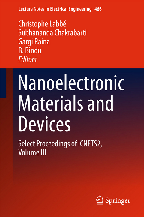
Nanoelectronic Materials and Devices (eBook)
XII, 246 Seiten
Springer Singapore (Verlag)
978-981-10-7191-1 (ISBN)
This book gathers a collection of papers by international experts that were presented at the International Conference on NextGen Electronic Technologies (ICNETS2-2016). ICNETS2 encompassed six symposia covering all aspects of the electronics and communications domains, including relevant nano/micro materials and devices. Highlighting the latest research on nanoelectronic materials and devices, the book offers a valuable guide for researchers, practitioners and students working in the core areas of functional electronics nanomaterials, nanocomposites for energy application, sensing and high strength materials and simulation of novel device design structures for ultra-low power applications.
Dr. Christophe Labbé is an Associate Professor at CIMAP Lab (Centre de Recherche sur les Ions, les Matériaux et la Photonique) at Caen, France in the engineering school ENSICAEN. He obtained his PhD on rare earth lasers at the Interdisciplinary Research Center Laser Ions at Caen in 1999. After a postgraduate position in Israel at the Laser Arava Laboratory of the Ben-Gurion University of the Negev, Israel on ionic matrix lasers pumped by diode, he became an assistant professor at the Laboratory of Optical Functions for Telecommunications (FOTON Lab) in Rennes, France in 2002. His ongoing research focuses on photon sources for telecommunications or visible light applications, and on photovoltaic cells.
Dr. Subhananda Chakrabarti received his MSc and PhD degrees from the Department of Electronic Science, University of Calcutta, India in 1993 and 2000, respectively. He was a Lecturer at the Department of Physics, St. Xavier's College, Kolkata. He served as a Senior Research Fellow with the University of Michigan, Ann Arbor, USA from 2001 to 2005, as a Senior Researcher with Dublin City University, Ireland, from 2005 to 2006, and as a Senior Researcher (RA2) with the University of Glasgow, UK, from 2006 to 2007. He became an Assistant Professor at the Department of Electrical Engineering, Indian Institute of Technology Bombay (IIT Bombay), India, in 2007, where he currently serves as a Professor. He is a Fellow of the Institution of Electrical and Telecommunication Engineers (IETE) India and a Member of the IEEE, MRS USA, SPIE USA etc. His research interests lie in compound (III-V and II-VI) semiconductor-based optoelectronic materials and devices.
Prof. (Dr.) Gargi Raina is a Professor at the School of Electronics Engineering (SENSE), VIT University, India. She completed her MS in Condensed Matter Physics at the Department of Physics and Astronomy, University of Hawaii at Manoa, USA (1991). She obtained her PhD from Jawaharlal Nehru Centre for Advanced Scientific Research (JNCASR), Bangalore, India in 2004. She worked as an 'Application Scientist' and helped set up the Advanced Metrology Application Lab of Digital Instruments/Veeco Inc., USA at JNCASR, Bangalore. She joined the Vellore Institute of Technology in 2006 as an Associate Professor and has been a Professor since 2008, while also serving as Director of the Center for Nanotechnology Research from June 2014 to September 2015. Her current research interests include functional nanomaterials, nanopatterning and assembly techniques, scanning probe microscopy (SPM)-based nanolithography, patterning and Lithography for graphene, graphene and nanocarbon materials for energy applications, simulation of carbon nanotube (CNT)/graphene-based nanoscale devices, and plasmonic nanolithography.
Dr. B. Bindu received her MTech in Digital Electronics from Cochin University of Science and Technology, India and Ph.D. in Electrical Engineering from the Indian Institute of Technology Madras (IIT Madras), Chennai, India. Her specialization is in nanoelectronics and very-large-scale integration (VLSI). She worked as a postdoctoral researcher for three years with the Device Modelling Group, University of Glasgow, UK and with the Institute for Microelectronics, Technical University Vienna, Austria. Currently, she is an Associate Professor at VIT University, Chennai. Her current research interests include the modelling of various issues in nanoscaled metal-oxide semiconductor field-effect transistors (MOSFETs), compact modelling of non-classical MOSFETs, and power semiconductor devices for analog and digital VLSI circuit design.
This book gathers a collection of papers by international experts that were presented at the International Conference on NextGen Electronic Technologies (ICNETS2-2016). ICNETS2 encompassed six symposia covering all aspects of the electronics and communications domains, including relevant nano/micro materials and devices. Highlighting the latest research on nanoelectronic materials and devices, the book offers a valuable guide for researchers, practitioners and students working in the core areas of functional electronics nanomaterials, nanocomposites for energy application, sensing and high strength materials and simulation of novel device design structures for ultra-low power applications.
Dr. Christophe Labbé is an Associate Professor at CIMAP Lab (Centre de Recherche sur les Ions, les Matériaux et la Photonique) at Caen, France in the engineering school ENSICAEN. He obtained his PhD on rare earth lasers at the Interdisciplinary Research Center Laser Ions at Caen in 1999. After a postgraduate position in Israel at the Laser Arava Laboratory of the Ben-Gurion University of the Negev, Israel on ionic matrix lasers pumped by diode, he became an assistant professor at the Laboratory of Optical Functions for Telecommunications (FOTON Lab) in Rennes, France in 2002. His ongoing research focuses on photon sources for telecommunications or visible light applications, and on photovoltaic cells. Dr. Subhananda Chakrabarti received his MSc and PhD degrees from the Department of Electronic Science, University of Calcutta, India in 1993 and 2000, respectively. He was a Lecturer at the Department of Physics, St. Xavier’s College, Kolkata. He served as a Senior Research Fellow with the University of Michigan, Ann Arbor, USA from 2001 to 2005, as a Senior Researcher with Dublin City University, Ireland, from 2005 to 2006, and as a Senior Researcher (RA2) with the University of Glasgow, UK, from 2006 to 2007. He became an Assistant Professor at the Department of Electrical Engineering, Indian Institute of Technology Bombay (IIT Bombay), India, in 2007, where he currently serves as a Professor. He is a Fellow of the Institution of Electrical and Telecommunication Engineers (IETE) India and a Member of the IEEE, MRS USA, SPIE USA etc. His research interests lie in compound (III-V and II-VI) semiconductor-based optoelectronic materials and devices. Prof. (Dr.) Gargi Raina is a Professor at the School of Electronics Engineering (SENSE), VIT University, India. She completed her MS in Condensed Matter Physics at the Department of Physics and Astronomy, University of Hawaii at Manoa, USA (1991). She obtained her PhD from Jawaharlal Nehru Centre for Advanced Scientific Research (JNCASR), Bangalore, India in 2004. She worked as an “Application Scientist” and helped set up the Advanced Metrology Application Lab of Digital Instruments/Veeco Inc., USA at JNCASR, Bangalore. She joined the Vellore Institute of Technology in 2006 as an Associate Professor and has been a Professor since 2008, while also serving as Director of the Center for Nanotechnology Research from June 2014 to September 2015. Her current research interests include functional nanomaterials, nanopatterning and assembly techniques, scanning probe microscopy (SPM)-based nanolithography, patterning and Lithography for graphene, graphene and nanocarbon materials for energy applications, simulation of carbon nanotube (CNT)/graphene-based nanoscale devices, and plasmonic nanolithography. Dr. B. Bindu received her MTech in Digital Electronics from Cochin University of Science and Technology, India and Ph.D. in Electrical Engineering from the Indian Institute of Technology Madras (IIT Madras), Chennai, India. Her specialization is in nanoelectronics and very-large-scale integration (VLSI). She worked as a postdoctoral researcher for three years with the Device Modelling Group, University of Glasgow, UK and with the Institute for Microelectronics, Technical University Vienna, Austria. Currently, she is an Associate Professor at VIT University, Chennai. Her current research interests include the modelling of various issues in nanoscaled metal-oxide semiconductor field-effect transistors (MOSFETs), compact modelling of non-classical MOSFETs, and power semiconductor devices for analog and digital VLSI circuit design.
Preface 6
Acknowledgements 7
Contents 8
About the Editors 10
1 The Effect of Functionalized MWCNT on Mechanical and Electrical Properties of PMMA Nanocomposites 12
Abstract 12
1 Introduction 13
2 Materials and Fabrication Technique 13
2.1 Materials 13
2.2 Functionalization of MWCNTs 13
2.3 Fabrication Method 14
2.4 Specimen Preparation 14
2.5 Testing of Specimens 15
3 Experimental Results 16
4 Conclusions 20
References 20
2 Performance Analysis of Dual Metal Double Gate Tunnel-FETs for Ultralow Power Applications 21
Abstract 21
1 Introduction 21
2 Structure Architecture and Parameter Description 22
3 Results and Discussion 24
3.1 Transfer Characteristics 24
3.2 Steeper Switching Behavior 24
3.3 Effects of Various Doping Concentrations 25
3.4 Effects of Different Oxide Thickness 25
4 Conclusion 26
Acknowledgements 26
References 26
3 Films of Reduced Graphene Oxide-Based Metal Oxide Nanoparticles 29
Abstract 29
1 Introduction 29
2 Experimental Details 30
2.1 Synthesis of rGO-Metal Oxide NP Films 30
3 Results and Discussion 31
4 Conclusion 36
References 37
4 Size Optimization of InAs/GaAs Quantum Dots for Longer Storage Memory Applications 38
Abstract 38
1 Introduction 38
2 Theoretical Model 39
3 Results and Discussions 41
4 Conclusion 43
Acknowledgements 43
References 44
5 Design and Analysis of a CMOS 180-nm Fractional-N Frequency Synthesizer 45
Abstract 45
1 Introduction 45
2 Fractional-N Frequency Synthesizer 46
3 Phase Frequency Detector (PFD) 46
4 Charge Pump 47
5 Loop Filter 47
6 Voltage Controlled Oscillator 48
7 Programmable Frequency Divider 50
7.1 Dual Modulus Prescaler 52
7.2 Integrated P & S Counter
8 Simulation Results 53
9 Conclusion 57
References 57
6 Memristor-Based Approximate Adders for Error Resilient Applications 58
Abstract 58
1 Introduction 59
2 Background 59
2.1 Mathematical Modeling of Memristor 59
2.2 Approximate Computing 60
3 Results and Discussion 60
3.1 1-Bit Full Adder 61
3.2 1-Bit Approximate Adder 62
3.3 4-Bit Ripple Carry Adder 62
3.4 Application in Image Processing 64
4 Conclusion 66
Acknowledgements 66
References 66
7 Integrated MEMS Capacitive Pressure Sensor with On-Chip CDC for a Wide Operating Temperature Range 67
Abstract 67
1 Introduction 68
2 Implementation and Design of the SiGe Pressure Sensor 70
2.1 Fundamentals of Octagonal Diaphragm 70
2.2 Structural Design of Octagonal SiGe Diaphragm 72
3 Design of Interface Electronics 73
3.1 CMOS Interface Circuit Design and Architecture 73
3.2 Detailed Design of CMOS Signal Conditioning Circuits 76
3.2.1 Constant-gm Biasing Circuit 76
3.2.2 Folded Cascode Amplifier 77
3.2.3 Comparator 77
4 Simulation Results and Discussions 79
4.1 Sensor Simulation Techniques 79
4.2 Circuit Simulation Techniques 84
5 Conclusion 84
Acknowledgements 85
References 85
8 A High SNDR and Wider Signal Bandwidth CT ?? Modulator with a Single Loop Nonlinear Feedback Compensation 86
Abstract 86
1 Introduction 86
2 Modulator Architecture 88
3 Circuit Implementation 89
3.1 Simulation Tool 89
3.2 Device-Level Implementation 89
3.2.1 Transconductance Amplifier Gm1 89
3.2.2 DACs 89
3.2.3 Transconductance Amplifiers Gm2, Gm3, GmF, and GmR 91
3.2.4 A 4-Bit Quantizer 92
4 Conclusion 94
Acknowledgements 94
References 95
9 Design of Current-Mode CNTFET Transceiver for Bundled Carbon Nanotube Interconnect 96
Abstract 96
1 Introduction 96
1.1 CNT Field-Effect Transistor 98
2 Current-Mode CNTFET Transceiver Design 98
2.1 Current-Mode Pseudo CNTFET Transmitter 99
2.2 CNTFET Clamped Interconnect Current Sense Amplifier 99
3 Performance Analysis 101
4 Test Setup 102
5 Conclusion 103
References 104
10 Weak Cell Detection Techniques for Memristor-Based Memories 106
Abstract 106
1 Introduction 107
2 Memristor-Based Memory 108
3 Memristor Memory: Defects and Faults 109
4 Memristor Memory: Testing Techniques 110
5 Proposed Weak Cell Detection Techniques 111
5.1 Low Write Voltage (LWV) 112
5.2 Short Write Time (SWT) 112
5.3 Short Refresh Time (SRT) 113
6 Conclusion 114
References 114
11 Enhancement of Transconductance Using Multi-Recycle Folded Cascode Amplifier 116
Abstract 116
1 Introduction 117
2 Conventional FC and RFC Structure 118
3 Proposed QRFC OTA Structure 120
3.1 Circuit Description 121
3.2 Equations and Mathematical Analysis 121
4 Simulation and Results 123
5 Conclusion 127
Acknowledgements 127
References 127
12 Nondestructive Read Circuit for Memristor-Based Memories 128
Abstract 128
1 Introduction 129
2 Memristor Write and Read Operations 130
2.1 Write Operation 130
2.2 Read Operation 130
3 Nondestructive Read Methods 132
4 Proposed Nondestructive Read Circuit 133
5 Simulation Results 134
6 Conclusion 135
References 136
13 A Built-in Self-Repair Architecture for Random Access Memories 137
Abstract 137
1 Introduction 137
2 Proposed Methodology 138
3 Review of SRAM 139
4 Failures in SRAM 139
4.1 Write Circuitry 140
4.2 Decoder 140
4.3 Circuit Under Test 141
4.4 Sense Amplifier 141
4.5 Switches 142
4.6 Fault Activator 143
4.7 Parallel Input Parallel Output 143
5 Functionality of SRAM 144
6 BISR Architecture 144
7 Simulation Results 147
8 Conclusion 149
Acknowledgements 149
References 149
14 A Current-Mode DC–DC Boost Converter with Fast Transient and On-Chip Current-Sensing Technique 151
Abstract 151
1 Introduction 151
2 Design Issues in Current-Mode Control 153
3 Circuit Implementation 155
3.1 Proposed OTA 155
3.1.1 Compensation 158
3.2 Current Sense 158
3.3 Comparator 160
3.4 Ramp Generator 161
3.5 Adder 162
3.6 PWM Generator 163
4 Measured Results 164
5 Conclusion 167
References 167
15 A Modified GDI-Based Low-Power and High Read Stability 8-T SRAM Memory with CNTFET Technology 169
Abstract 169
1 Introduction 170
2 Gate Diffusion Input (GDI) and Modified GDI Tecnique 170
3 8-T SRAM Cell Using CNTFET and M-GDI Technique 173
4 Simulation Results 175
5 Stability Analysis with Butterfly Curve 176
6 Conclusion 177
References 177
To Refer a Research Article 177
To Refer a Publication of Proceedings 178
Internet Source 178
16 High Performance Trench Gate Power MOSFET of Indium Phosphide 179
Abstract 179
1 Introduction 179
2 The Device Structure 180
3 Simulation Details 181
4 Results and Discussion 181
4.1 ON-State Performance 182
4.2 OFF-State Performance 183
4.3 Gate Capacitance 183
5 Conclusion 184
References 184
17 Memristor Equipped Error Detection Technique 186
Abstract 186
1 Introduction 187
2 Voltage Threshold Adaptive Memristor (VTEAM) Model 187
3 Error Detection Technique 189
4 Results and Discussion 192
5 Conclusion 193
References 194
18 28 nm FD-SOI SRAM Design Using Read Stable Bit Cell Architecture 195
Abstract 195
1 Introduction 196
2 Conventional SRAM Array 196
3 Previous Bit Cell Designs 198
4 Proposed Design 200
4.1 Design Consideration 200
4.2 Write Operation 201
4.3 Read Operation 202
5 Sense Amplifier 203
5.1 Considered Designs 203
6 Decoder Design 205
7 Simulation Results 206
7.1 Bit Cell Simulation Results 206
7.2 Sense Amplifier Simulation Results 206
7.3 Decoder Simulation Results 207
8 Conclusion 207
Acknowledgements 207
References 207
19 Design and Verification of Memory Controller with Host Wishbone Interface 209
Abstract 209
1 Introduction 209
2 Traditional Implementation Details of the Memory Controller 210
3 Memory Controller Architecture 211
3.1 Refresh Controller 211
3.2 Open Bank and Row Tracking 212
3.3 Address Mux and Counter 212
3.4 Configuration and Status Registers 212
3.5 Power on Configuration 212
3.6 Data Latch, Packer, and Parity 212
3.7 Memory Timing Controller and Memory Interface 213
4 Memory Controller Design Requirements 213
4.1 Wishbone Interface 213
4.2 Memory-Specific Requirements 214
5 Memory Timing Configuration 214
5.1 SDRAM Timing Configuration 214
5.2 SSRAM Timing Configuration 215
5.3 Synchronous Chip Select Devices 216
6 Configuration and Status Registers 217
7 Final Design Implementation, Timing Details, and Design Summary 219
8 Memory Controller Verification Flow 220
8.1 Features Listing Down 220
8.2 Test Plan Development 221
8.3 Functional Coverage Point Listing Down 221
8.4 Test Bench Architecture Definition 222
8.5 Test Bench Component Coding and Coverage Reports 223
9 Results and Discussion 223
10 Conclusion 232
References 233
20 8-Bit Asynchronous Wave-Pipelined Arithmetic Logic Unit 234
Abstract 234
1 Introduction 234
2 ALU Architecture 235
2.1 Kogge–Stone Adder 235
2.2 Wave-Pipelined Architecture 236
2.3 Internal Modules of Existing 237
2.3.1 INIT Module 237
2.3.2 ROUT1 Module 237
2.3.3 ROUT2 Module 239
2.3.4 SUM Module 239
2.4 Internal Modules of Modified ALU 240
2.4.1 INIT Module 240
2.4.2 ROUT1 Module 241
2.4.3 ROUT2 Module 241
2.4.4 SUM Module 242
3 Results and Discussion 243
4 Conclusion 244
References 244
Author Index 245
| Erscheint lt. Verlag | 27.11.2017 |
|---|---|
| Reihe/Serie | Lecture Notes in Electrical Engineering | Lecture Notes in Electrical Engineering |
| Zusatzinfo | XII, 246 p. 197 illus., 73 illus. in color. |
| Verlagsort | Singapore |
| Sprache | englisch |
| Themenwelt | Technik ► Elektrotechnik / Energietechnik |
| Technik ► Maschinenbau | |
| Schlagworte | Computational Nanoelectronics Magnetic nanomaterials • Functional Electronic Nanomaterials • MEMS Nanomaterials for batteries and supercapacitors • Nanoelectronic Devices, Nanosensors • Nanoelectronic materials for Energy application • Spintronics |
| ISBN-10 | 981-10-7191-8 / 9811071918 |
| ISBN-13 | 978-981-10-7191-1 / 9789811071911 |
| Haben Sie eine Frage zum Produkt? |
Größe: 10,9 MB
DRM: Digitales Wasserzeichen
Dieses eBook enthält ein digitales Wasserzeichen und ist damit für Sie personalisiert. Bei einer missbräuchlichen Weitergabe des eBooks an Dritte ist eine Rückverfolgung an die Quelle möglich.
Dateiformat: PDF (Portable Document Format)
Mit einem festen Seitenlayout eignet sich die PDF besonders für Fachbücher mit Spalten, Tabellen und Abbildungen. Eine PDF kann auf fast allen Geräten angezeigt werden, ist aber für kleine Displays (Smartphone, eReader) nur eingeschränkt geeignet.
Systemvoraussetzungen:
PC/Mac: Mit einem PC oder Mac können Sie dieses eBook lesen. Sie benötigen dafür einen PDF-Viewer - z.B. den Adobe Reader oder Adobe Digital Editions.
eReader: Dieses eBook kann mit (fast) allen eBook-Readern gelesen werden. Mit dem amazon-Kindle ist es aber nicht kompatibel.
Smartphone/Tablet: Egal ob Apple oder Android, dieses eBook können Sie lesen. Sie benötigen dafür einen PDF-Viewer - z.B. die kostenlose Adobe Digital Editions-App.
Zusätzliches Feature: Online Lesen
Dieses eBook können Sie zusätzlich zum Download auch online im Webbrowser lesen.
Buying eBooks from abroad
For tax law reasons we can sell eBooks just within Germany and Switzerland. Regrettably we cannot fulfill eBook-orders from other countries.
aus dem Bereich


