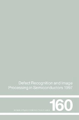
Defect Recognition and Image Processing in Semiconductors 1997
Proceedings of the seventh conference on Defect Recognition and Image Processing, Berlin, September 1997
Seiten
1998
Institute of Physics Publishing (Verlag)
978-0-7503-0500-6 (ISBN)
Institute of Physics Publishing (Verlag)
978-0-7503-0500-6 (ISBN)
Presents an overview of techniques used to assess, monitor, and characterize defects from the atomic scale to inhomogeneities in complete silicon wafers. This book addresses advances in defect analyzing techniques and instrumentation and their application to substrates, epilayers, and devices. It investigates defects in layers and devices.
Defect Recognition and Image Processing in Semiconductors 1997 provides a valuable overview of current techniques used to assess, monitor, and characterize defects from the atomic scale to inhomogeneities in complete silicon wafers. This volume addresses advances in defect analyzing techniques and instrumentation and their application to substrates, epilayers, and devices. The book discusses the merits and limits of characterization techniques; standardization; correlations between defects and device performance, including degradation and failure analysis; and the adaptation and application of standard characterization techniques to new materials. It also examines the impressive advances made possible by the increase in the number of nanoscale scanning techniques now available. The book investigates defects in layers and devices, and examines the problems that have arisen in characterizing gallium nitride and silicon carbide.
Defect Recognition and Image Processing in Semiconductors 1997 provides a valuable overview of current techniques used to assess, monitor, and characterize defects from the atomic scale to inhomogeneities in complete silicon wafers. This volume addresses advances in defect analyzing techniques and instrumentation and their application to substrates, epilayers, and devices. The book discusses the merits and limits of characterization techniques; standardization; correlations between defects and device performance, including degradation and failure analysis; and the adaptation and application of standard characterization techniques to new materials. It also examines the impressive advances made possible by the increase in the number of nanoscale scanning techniques now available. The book investigates defects in layers and devices, and examines the problems that have arisen in characterizing gallium nitride and silicon carbide.
Doneker, J.
Preface. Glossary. Nanoscanning (9 papers). Electron beam methods (9 papers). Optical methods (8 papers). Mapping (10 papers). X-ray methods (4 papers). Other and combined methods (8 papers). Image processing. Standardization. Si and SiGe mixed crystals (15 papers). SiC (3 papers). GaN (6 papers). Other III-V compounds (12 papers). II-VI compounds, phosphors, oxides and alternative substrates (4 papers). Processing and defects (3 papers). Defect recognition in devices and degradation (11 papers). Author and subject indices.
| Erscheint lt. Verlag | 1.1.1998 |
|---|---|
| Reihe/Serie | Institute of Physics Conference Series |
| Verlagsort | London |
| Sprache | englisch |
| Maße | 156 x 234 mm |
| Gewicht | 975 g |
| Themenwelt | Naturwissenschaften ► Physik / Astronomie ► Festkörperphysik |
| Technik ► Elektrotechnik / Energietechnik | |
| Technik ► Maschinenbau | |
| ISBN-10 | 0-7503-0500-2 / 0750305002 |
| ISBN-13 | 978-0-7503-0500-6 / 9780750305006 |
| Zustand | Neuware |
| Haben Sie eine Frage zum Produkt? |
Mehr entdecken
aus dem Bereich
aus dem Bereich


