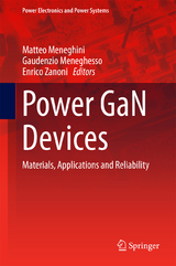
Power GaN Devices (eBook)
X, 380 Seiten
Springer International Publishing (Verlag)
978-3-319-43199-4 (ISBN)
This book presents the first comprehensive overview of the properties and fabrication methods of GaN-based power transistors, with contributions from the most active research groups in the field. It describes how gallium nitride has emerged as an excellent material for the fabrication of power transistors; thanks to the high energy gap, high breakdown field, and saturation velocity of GaN, these devices can reach breakdown voltages beyond the kV range, and very high switching frequencies, thus being suitable for application in power conversion systems. Based on GaN, switching-mode power converters with efficiency in excess of 99 % have been already demonstrated, thus clearing the way for massive adoption of GaN transistors in the power conversion market. This is expected to have important advantages at both the environmental and economic level, since power conversion losses account for 10 % of global electricity consumption.
The first part of the book describes the properties and advantages of gallium nitride compared to conventional semiconductor materials. The second part of the book describes the techniques used for device fabrication, and the methods for GaN-on-Silicon mass production. Specific attention is paid to the three most advanced device structures: lateral transistors, vertical power devices, and nanowire-based HEMTs. Other relevant topics covered by the book are the strategies for normally-off operation, and the problems related to device reliability. The last chapter reviews the switching characteristics of GaN HEMTs based on a systems level approach.
This book is a unique reference for people working in the materials, device and power electronics fields; it provides interdisciplinary information on material growth, device fabrication, reliability issues and circuit-level switching investigation.
Matteo Meneghini received the Ph.D. degree in the optimization of GaN-based LED and laser structures from the University of Padova, Italy. He is currently Assistant Professor at the Department of Information Engineering, University of Padova. During his career he has extensively worked on the reliability and parasitics of GaN-based semiconductor devices for application in the RF, power electronics and optoelectronics fields: his research is mainly focused towards the understanding of the physical mechanisms that limit the performance and the reliability of GaN-based LEDs, lasers, and HEMTs.
Gaudenzio Meneghesso received the Ph.D. degree in electrical and telecommunication engineering from the University of Padova, Padova, Italy, in 1997. In 1995, he was with the University of Twente, Enschede, The Netherlands, with a Human Capital and Mobility fellowship (within the SUSTAIN Network) working on the dynamic behavior of protection structures against electrostatic discharge (ESD). Since 2011, he has been a Full Professor with the Department of Information Engineering, University of Padova.
Enrico Zanoni was born in Verona, Italy, in 1956. He received the Laurea degree in physics (cum laude) from the University of Modena and Reggio Emilia, Modena, Italy, in 1982, after a student internship with the S. Carlo Foundation, Modena. During 1985-1988, he was an Assistant Professor with the Faculty of Engineering, University of Bari, Bari, Italy. From 1988 to 1993, he frequently visited the U.S. and established research collaborations with Bell Laboratories; Hughes Research Laboratories; IBM T. J. Watson Research Center; Massachusetts Institute of Technology, Cambridge, MA, USA; TRW (currently, Northrop Grumman); University of California, Santa Barbara, CA, USA; and many other industrial and academic laboratories. During 1996-1997, he was a Full Professor of industrial electronics with the University of Modena and Reggio Emilia. He is currently with the University of Padova, Padua, Italy, where he was an Assistant Professor during 1988-1992, an Associate Professor of electronics during 1992-1993, a Full Professor of microelectronics during 1993-1996, and has been a Full Professor of digital electronics with the Department of Information Engineering since 1997.
Matteo Meneghini received the Ph.D. degree in the optimization of GaN-based LED and laser structures from the University of Padova, Italy. He is currently Assistant Professor at the Department of Information Engineering, University of Padova. During his career he has extensively worked on the reliability and parasitics of GaN-based semiconductor devices for application in the RF, power electronics and optoelectronics fields: his research is mainly focused towards the understanding of the physical mechanisms that limit the performance and the reliability of GaN-based LEDs, lasers, and HEMTs. Gaudenzio Meneghesso received the Ph.D. degree in electrical and telecommunication engineering from the University of Padova, Padova, Italy, in 1997. In 1995, he was with the University of Twente, Enschede, The Netherlands, with a Human Capital and Mobility fellowship (within the SUSTAIN Network) working on the dynamic behavior of protection structures against electrostatic discharge (ESD). Since 2011, he has been a Full Professor with the Department of Information Engineering, University of Padova.Enrico Zanoni was born in Verona, Italy, in 1956. He received the Laurea degree in physics (cum laude) from the University of Modena and Reggio Emilia, Modena, Italy, in 1982, after a student internship with the S. Carlo Foundation, Modena. During 1985–1988, he was an Assistant Professor with the Faculty of Engineering, University of Bari, Bari, Italy. From 1988 to 1993, he frequently visited the U.S. and established research collaborations with Bell Laboratories; Hughes Research Laboratories; IBM T. J. Watson Research Center; Massachusetts Institute of Technology, Cambridge, MA, USA; TRW (currently, Northrop Grumman); University of California, Santa Barbara, CA, USA; and many other industrial and academic laboratories. During 1996–1997, he was a Full Professor of industrial electronics with the University of Modena and Reggio Emilia. He is currently with the University of Padova, Padua, Italy, where he was an Assistant Professor during 1988–1992, an Associate Professor of electronics during 1992–1993, a Full Professor of microelectronics during 1993–1996, and has been a Full Professor of digital electronics with the Department of Information Engineering since 1997.
Preface 6
Contents 9
1 Properties and Advantages of Gallium Nitride 11
1.1 General Background 11
1.2 GaN Material 12
1.3 Polarization Effect 16
1.4 GaN-Based FET 19
1.5 Natural Super Junction (NSJ) Structure 21
1.6 On-Resistance and Breakdown Voltage 24
1.7 Low-Voltage Devices 25
1.8 High-Voltage Devices 29
1.9 Future Study in GaN Vertical Power Device 33
References 35
2 Substrates and Materials 37
2.1 Substrate Overview 38
2.2 Metal-Organic Chemical Vapor Deposition 40
2.2.1 Fabrication of Semi-insulating (S.I.) (Al,Ga)N Layers 42
2.2.2 n- and p-Type Doping 43
2.2.3 AlGaN/GaN Heterostructures 44
2.3 Traps and Dispersion 45
2.4 Fabrication of Epitaxial Structures for Lateral Power Switching Devices 45
2.4.1 Current-Blocking Layer Deposition on Silicon Substrates 47
2.4.2 Current-Blocking Layer Deposition on Silicon Carbide Substrates 48
2.4.3 Current Blocking Layer Deposition on Sapphire Substrates 48
2.4.4 Gating Layer Growth 50
2.5 Vertical Devices 50
2.6 Outlook 55
2.6.1 InAlN and AlInGaN Barrier Layers 55
2.6.2 Devices Based on Non-c-plane GaN 56
References 57
3 GaN-on-Silicon CMOS-Compatible Process 63
3.1 GaN-on-Si Epitaxy 63
3.2 GaN-on-Si Au-Free Processing 65
3.3 Au-Free Ohmic Contact 69
3.3.1 AlGaN Barrier Recess 71
3.3.2 Ohmic Alloy Optimization 71
3.3.3 Ti/Al Ratio 72
3.3.4 Si Layer at Bottom of Ohmic Metal Stack 73
3.4 Gallium Contamination Issues 74
3.5 Conclusion 77
References 77
4 Lateral GaN Devices for Power Applications (from kHz to GHz) 79
4.1 Introduction 79
4.2 History of AlGaN/GaN HEMTs 79
4.3 Addressing Dispersion 81
4.4 Gallium Nitride for mm-Wave Applications 84
4.5 Historical Perspective of N-Polar GaN Development 86
4.6 GaN Applied to Power Electronics 95
4.7 Conclusions 102
Acknowledgments 103
References 103
5 Vertical Gallium Nitride Technology 110
5.1 Introduction 110
5.2 Device Topology 112
5.2.1 Vertical Devices Versus Lateral Devices 112
5.3 Evolution of a CAVET 114
5.4 Design of a CAVET 117
5.4.1 A Discussion of the Key Components Required for the Successful Functioning of the Device 117
5.5 The Key Components of a CAVET 119
5.5.1 Current Blocking Layers 124
5.5.2 Performance and Cost 126
5.6 Role of Bulk GaN Substrate 127
5.7 CAVETs for RF Application 128
5.8 Conclusion 128
Acknowledgments 129
References 129
6 GaN-Based Nanowire Transistors 131
6.1 Introduction 131
6.1.1 Bottom-Up Nanowire Devices: GaN Nanowire Field-Effect Transistors 133
6.1.2 Top-Down Nanowire Devices 135
6.1.2.1 Tri-Gate GaN Transistors for Power Electronics Applications 135
6.2 Tri-Gate GaN Power MISFET 135
6.2.1 Additional Considerations of Tri-gate GaN Power Transistors 139
6.3 Nanowires for RF Applications: Increasing Linearity of Gm 142
6.4 Nanostructured GaN Schottky Barrier Diodes 145
6.4.1 Nanostructured Anode for GaN SBDs 145
6.5 Conclusions 148
References 150
7 Deep-Level Characterization: Electrical and Optical Methods 153
7.1 Introduction 153
7.2 Fundamentals of DLTS and DLOS 155
7.2.1 C-DLTS 155
7.2.2 C-DLOS 157
7.2.3 Applicability of C-DLTS and C-DLOS to HEMTs 158
7.2.4 I-DLTS and I-DLOS 159
7.3 Application of DLTS and DLOS to GaN HEMTs 161
7.3.1 Using Fill Pulses to Spatially Locate Traps 162
7.3.2 Using Measurement Bias to Spatially Locate Traps 166
7.3.3 Additional Methods to Measure Spatially Localized Traps 168
7.4 Conclusion 169
References 170
8 Modelling of GaN HEMTs: From Device-Level Simulation to Virtual Prototyping 172
8.1 Introduction 172
8.2 Device-Level Simulation 174
8.2.1 Pulsed Mode Behavior 177
8.3 Non-optimized Buffer Technology 177
8.4 Optimized Buffer Technology 181
8.4.1 AC Capacitances 183
8.4.2 Off-state Breakdown 185
8.5 Spice Model Development and Calibration 187
8.6 Application Board Characterization and Simulations 189
8.6.1 Normally-off pGaN Transistors 192
8.6.2 Normally-on HEMT: Cascode Design 195
8.7 Conclusions 201
References 201
9 Performance-Limiting Traps in GaN-Based HEMTs: From Native Defects to Common Impurities 204
9.1 Surface-Related Trapping 209
9.2 Impact of Iron Doping 212
9.2.1 Properties of Deep Level E2 and Impact of Iron Doping 212
9.2.2 Origin of the Trap E2 215
9.2.3 Impact of Electrical Stress on Trapping Mechanisms 217
9.3 Impact of Carbon Doping 219
9.4 Trapping Mechanisms in Metal Insulator Semiconductor High-Electron-Mobility Transistors (MIS-HEMTs) 226
9.4.1 Origin of the Trapping Induced by Positive Gate Bias 227
9.4.2 Analysis of Fast and Slow Trapping Mechanisms 230
9.4.3 Materials and Deposition Techniques for the Improvement of Trapping Effects 230
References 234
10 Cascode Gallium Nitride HEMTs on Silicon: Structure, Performance, Manufacturing, and Reliability 244
10.1 Motivation and Configuration of the Cascode GaN HEMT 244
10.2 Functionality and Benefits of Cascode GaN HEMT 245
10.3 Key Applications and Performance Advantage of Cascode GaN HEMTs 246
10.3.1 Diode-Free Half-Bridge Architecture 246
10.3.2 Gate-Drive Considerations 247
10.4 Products in the Market 249
10.5 Applications and Key Performance Benefits 250
10.5.1Totem-Pole Power Factor Correction Circuit (PFC) 250
10.5.2 PV Inverters 251
10.5.3 All-in-One Power Supplies with GaN AC–DC PFC and Full-Bridge Resonant Switching LLC DC–DC Con ... 251
10.6 Qualification and Reliability of Cascode GaN HEMTs 253
10.6.1 JEDEC Qualification 254
10.6.2 Extended Qualification/Reliability Testing 255
10.6.3 Operating and Intrinsic Lifetime Testing 256
10.7 Manufacturing Excellence 258
10.8 On Single-Chip e-Mode GaN 259
10.9 Future Outlook 260
10.9.1 Next-Generation Products 260
10.9.2 Intellectual Property Considerations 260
10.9.3 In Summary 260
Acknowledgments 261
References 261
11 Gate Injection Transistors: E-mode Operation and Conductivity Modulation 262
11.1Operation Principle of GIT 262
11.2DC and Switching Performances ofGIT 263
11.3 State-of-the-Art Reliability of GIT 268
11.4 Applications ofGIT to Practical Switching Systems 270
11.5 Advanced Technologies ofGIT for Future Power Electronics 275
11.6 Summary 278
Acknowledgments 278
References 279
12 Fluorine-Implanted Enhancement-Mode Transistors 280
12.1 Introduction: Fluorine in III-Nitride Heterostructures: Robust Vth Control 280
12.2 Physics Mechanism of Fluorine Implantation 282
12.2.1 Atomistic Modeling of F Plasma Ion Implantation 282
12.2.2 Stability of F Ions in AlGaN/GaN Heterostructures 284
12.2.3 Electron Binding Energy Around F Ions 287
12.3 Fluorine-Implanted Enhancement-Mode GaN MIS-HEMTs 288
12.3.1 GaN MIS-HEMTs 288
12.3.2 GaN MIS-HEMTs with Partially Recessed Fluorine-Implanted Barrier 291
12.3.3 GaN Smart Power ICs 293
12.4 Conclusions 298
Acknowledgments 298
References 299
13 Drift Effects in GaN High-Voltage Power Transistors 301
13.1 Introduction 301
13.2 Drift Effects and Their Physical Mechanisms 302
13.2.1 Overview 302
13.2.2 Basic Physical Understanding 302
13.2.3 Dependency on Device Operation Conditions 305
13.3 Drift Phenomena in GaN Power Switching Transistors 306
13.3.1 Dynamic On-State Resistance (Ron_dyn) 306
13.3.1.1 Power Switching from Off-State Bias Point 307
13.3.1.2 Trapping Effects During On-State Operation 313
13.3.2Threshold Voltage Shift 313
13.3.3Kink Effect 314
13.4 Technological Countermeasures 316
13.4.1 Optimized Epitaxial Buffer Design 317
13.4.2 Reduction of Electrical Field in Critical Device Regions 318
Acknowledgments 320
References 320
14 Reliability Aspects of 650-V-Rated GaN Power Devices 324
14.1 Introduction 324
14.2Reliability of Au-Free Ohmic Contacts 324
14.2.1 Introduction to Ohmic Contact Reliability 324
14.2.2 Au-Free Ohmic Contacts Processing 325
14.2.3 Stressing and Measurement Procedure 326
14.2.4Reliability Evaluation of Au-Free Ohmic Contacts 328
14.2.4.1 Degradation as a Function of Contact Spacing 328
14.2.4.2 Degradation as a Function of Stress Power 328
14.2.4.3 Temperature Dependence and Activation Energy 330
14.2.4.4 Failure Mechanisms 332
14.2.5 Conclusions 334
14.3 Intrinsic Reliability of MISHEMT Gate Dielectrics 334
14.3.1 Introduction 334
14.3.2 Experiments 335
14.3.3 Analysis of Leakage Current Under Forward Bias Condition 336
14.3.4 Analysis of Leakage Current Under Reverse Bias Condition 339
14.3.5 Analysis of Defect States in Bulk SiN 340
14.3.6 TDDB Study 340
14.3.7 Conclusions 343
14.4 Buffer Stack Reliability—Off-State High-Voltage Drain Stress 343
14.4.1 Introduction 343
14.4.2 Current Conduction Mechanism 344
14.4.3 High-Temperature Reverse Bias 344
14.4.4 High-Voltage off-State Drain Stress 346
14.4.5 Conclusions 347
References 348
15 Switching Characteristics of Gallium Nitride Transistors: System-Level Issues 350
15.1 Switching Characteristics of E-mode and Cascode GaN 351
15.1.1 Switching Loss Mechanism 351
15.1.2 Packaging Influence 352
15.1.3 Comparison Between Hard Switching and Soft Switching 356
15.2 Special Issues of Cascode GaN 357
15.2.1 Impact of Packaging on Gate Breakdown 357
15.2.2 Impact of Capacitor Mismatch 358
15.2.2.1 Si Avalanche 358
15.2.2.2 Failure to Achieve ZVS 360
15.2.2.3 Divergent Oscillation 361
15.2.2.4 Solution to Solve Capacitor Mismatch Issue 363
15.3 Gate Driver Design for GaN Device 364
15.3.1 The di/dt Issue 364
15.3.2 The dv/dt Issue 365
15.4 System-Level Impact 368
15.4.1 3D Integrated Point-of-Load Converter 368
15.4.2 Isolated DC/DC Converter 371
15.4.2.1 48–12 V DCX 371
15.4.2.2 400–12 V DCX 372
15.4.3 MHz Totem-Pole PFC Rectifier 374
15.4.4High-Density Wall Adapter 377
15.5 Summary 378
References 379
Author index 381
Subject index 382
| Erscheint lt. Verlag | 8.9.2016 |
|---|---|
| Reihe/Serie | Power Electronics and Power Systems | Power Electronics and Power Systems |
| Zusatzinfo | X, 380 p. 306 illus., 266 illus. in color. |
| Verlagsort | Cham |
| Sprache | englisch |
| Themenwelt | Technik ► Elektrotechnik / Energietechnik |
| Technik ► Maschinenbau | |
| Schlagworte | Gallium nitride on silicon (GaN-on-Si) • Gallium nitride power transistors • GaN-based nanowire transistors • GaN-based power transistors • GaN-based vertical transistors • Lateral GaN-based power devices • Nanowire-based HEMTs • Normally-off devices • Power GaN device reliability • Single and double heterostructure devices |
| ISBN-10 | 3-319-43199-4 / 3319431994 |
| ISBN-13 | 978-3-319-43199-4 / 9783319431994 |
| Informationen gemäß Produktsicherheitsverordnung (GPSR) | |
| Haben Sie eine Frage zum Produkt? |
Größe: 25,9 MB
DRM: Digitales Wasserzeichen
Dieses eBook enthält ein digitales Wasserzeichen und ist damit für Sie personalisiert. Bei einer missbräuchlichen Weitergabe des eBooks an Dritte ist eine Rückverfolgung an die Quelle möglich.
Dateiformat: PDF (Portable Document Format)
Mit einem festen Seitenlayout eignet sich die PDF besonders für Fachbücher mit Spalten, Tabellen und Abbildungen. Eine PDF kann auf fast allen Geräten angezeigt werden, ist aber für kleine Displays (Smartphone, eReader) nur eingeschränkt geeignet.
Systemvoraussetzungen:
PC/Mac: Mit einem PC oder Mac können Sie dieses eBook lesen. Sie benötigen dafür einen PDF-Viewer - z.B. den Adobe Reader oder Adobe Digital Editions.
eReader: Dieses eBook kann mit (fast) allen eBook-Readern gelesen werden. Mit dem amazon-Kindle ist es aber nicht kompatibel.
Smartphone/Tablet: Egal ob Apple oder Android, dieses eBook können Sie lesen. Sie benötigen dafür einen PDF-Viewer - z.B. die kostenlose Adobe Digital Editions-App.
Zusätzliches Feature: Online Lesen
Dieses eBook können Sie zusätzlich zum Download auch online im Webbrowser lesen.
Buying eBooks from abroad
For tax law reasons we can sell eBooks just within Germany and Switzerland. Regrettably we cannot fulfill eBook-orders from other countries.
aus dem Bereich


