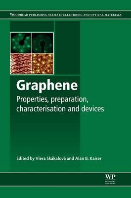
Graphene
Woodhead Publishing Ltd (Verlag)
978-0-08-101336-6 (ISBN)
- Titel erscheint in neuer Auflage
- Artikel merken
Chapters in part one explore the preparation of , including epitaxial growth of graphene on silicon carbide, chemical vapor deposition (CVD) growth of graphene films, chemically derived graphene, and graphene produced by electrochemical exfoliation. Part two focuses on the characterization of graphene using techniques including transmission electron microscopy (TEM), scanning tunneling microscopy (STM), and Raman spectroscopy. These chapters also discuss photoemission of low dimensional carbon systems. Finally, chapters in part three discuss electronic transport properties of graphene and graphene devices. This part highlights electronic transport in bilayer graphene, single charge transport, and the effect of adsorbents on electronic transport in graphene. It also explores graphene spintronics and nano-electro-mechanics (NEMS).
Graphene is a comprehensive resource for academics, materials scientists, and electrical engineers working in the microelectronics and optoelectronics industries.
Viera Skakalova works for the Faculty of Physics, University of Vienna, Austria. Alan Kaiser is Emeritus Professor at the School of Chemical and Physical Sciences and MacDiarmid Institute for Advanced Materials and Nanotechnology, Victoria University of Wellington, New Zealand.
Contributor contact details
Woodhead Publishing Series in Electronic and Optical Materials
Preface
Part I: Preparation of graphene
1. Epitaxial growth of graphene on silicon carbide (SiC)
Abstract:
1.1 Introduction
1.2 Ultrahigh vacuum (UHV) thermal decomposition of single-crystal SiC
1.3 Thermal decomposition of single-crystal SiC under ambient pressure conditions
1.4 Thermal decomposition of single-crystal SiC thin films and polycrystalline SiC substrates
1.5 Epitaxial graphene formed by intercalation
1.6 Conclusion
1.7 Acknowledgements
1.8 References
2. Chemical vapor deposition (CVD) growth of graphene films
Abstract:
2.1 Introduction
2.2 Chemical vapor deposition (CVD) on nickel
2.3 Graphene with large domain sizes on copper
2.4 Growth on copper single crystals
2.5 Periodically stacked multilayers
2.6 Isotope labeling of CVD graphene
2.7 Conclusion
2.8 Acknowledgment
2.9 References
3. Chemically derived graphene
Abstract:
3.1 Introduction
3.2 Synthesis of graphene oxide (GO)
3.3 Reduction of graphene oxide (GO)
3.4 Physicochemical structure of graphene oxide (GO)
3.5 Electrical transport in graphene oxide (GO)
3.6 Applications of graphene oxide/reduced graphene oxide (GO/RGO)
3.7 Conclusion
3.8 Acknowledgements
3.9 References
4. Graphene produced by electrochemical exfoliation
Abstract:
4.1 Introduction
4.2 Synthesis of graphene by electrochemical exfoliation: a basic concept
4.3 Applications of graphene and graphene-based materials
4.4 Conclusion
4.5 Acknowledgments
4.6 References
Part II: Characterisation of graphene
5. Transmission electron microscopy (TEM) of graphene
Abstract:
5.1 Introduction
5.2 Graphene structure basics
5.3 Electron diffraction analysis of graphene
5.4 Graphene and defects in graphene observed by aberration-corrected transmission electron microscopy (TEM) and scanning transmission electron microscopy (STEM)
5.5 Insights from electron microscopic studies of graphene
5.6 Conclusion
5.7 References
6. Scanning tunneling microscopy (STM) of graphene
Abstract:
6.1 Introduction
6.2 Morphology, perfection and electronic structure of graphene flakes deposited on inert substrates
6.3 Morphology, perfection and electronic structure of graphene epitaxially grown on semiconductor and metallic substrates
6.4 Scanning tunneling microscopy (STM)/scanning tunneling spectroscopy (STS) of point defects
6.5 STM/STS on graphene nanoribbons (GNR)
6.6 Conclusion
6.7 References
7. Raman spectroscopy of graphene
Abstract:
7.1 Introduction
7.2 Principles of Raman scattering
7.3 Phonons in graphene
7.4 Electronic structure of graphene
7.5 Raman spectrum of graphene
7.6 Conclusion
7.7 Acknowledgement
7.8 References
8. Photoemission of low-dimensional carbon systems
Abstract:
8.1 Introduction
8.2 Photoemission spectroscopy
8.3 Accessing the electronic properties of carbon sp2 hybridized systems: the C1s core level
8.4 Chemical state identification: inspection of bonding environments
8.5 Valence-band electronic structure
8.6 Conclusion
8.7 Acknowledgements
8.8 References
Part III: Electronic transport properties of graphene and graphene devices
9. Electronic transport in graphene: towards high mobility
Abstract:
9.1 Introduction
9.2 Metrics for scattering strength
9.3 Methods of graphene synthesis
9.4 Sources of scattering in graphene
9.5 Approaches to increase carrier mobility
9.6 Physical phenomena in high-mobility graphene
9.7 Conclusion
9.8 Acknowledgments
9.9 References
10. Electronic transport in bilayer graphene
Abstract:
10.1 Introduction
10.2 Historical development of bilayer graphene
10.3 Transport properties in bilayer graphene systems
10.4 Many-body effects of transport properties in bilayer graphene
10.5 Conclusion
10.6 References
11. Effect of adsorbents on electronic transport in graphene
Abstract:
11.1 Introduction
11.2 Interaction of adsorbates with graphene
11.3 Transfer-induced metal and molecule adsorptions
11.4 Influence of adsorbates on graphene field-effect transistors
11.5 Removal of polymer residues on graphene
11.6 Conclusion
11.7 References
12. Single-charge transport in graphene
Abstract:
12.1 Introduction
12.2 Single-charge tunneling
12.3 Electrical properties of graphene
12.4 Single-charge tunneling in graphene
12.5 Charge localization in graphene
12.6 Conclusion
12.7 References
13. Graphene spintronics
Abstract:
13.1 Introduction
13.2 Theories and important concepts
13.3 Experiments for generating pure spin current and the physical properties of pure spin current
13.4 Conclusion and future trends
13.5 References
14. Graphene nanoelectromechanics (NEMS)
Abstract:
14.1 Introduction
14.2 Graphene versus silicon
14.3 Graphene mechanical attributes
14.4 Fabrication technology for graphene microelectromechanical systems (MEMS)
14.5 Graphene nanoresonators
14.6 Graphene nanomechanical sensors
14.7 Conclusion and future trends
14.8 References
Index
| Erscheinungsdatum | 08.07.2016 |
|---|---|
| Reihe/Serie | Woodhead Publishing Series in Electronic and Optical Materials |
| Verlagsort | Cambridge |
| Sprache | englisch |
| Maße | 156 x 234 mm |
| Themenwelt | Technik ► Elektrotechnik / Energietechnik |
| Technik ► Maschinenbau | |
| ISBN-10 | 0-08-101336-1 / 0081013361 |
| ISBN-13 | 978-0-08-101336-6 / 9780081013366 |
| Zustand | Neuware |
| Haben Sie eine Frage zum Produkt? |
aus dem Bereich
