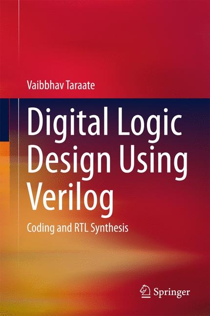
Digital Logic Design Using Verilog (eBook)
XXIII, 416 Seiten
Springer India (Verlag)
978-81-322-2791-5 (ISBN)
Vaibbhav Taraate is Entrepreneur and Mentor at 'Semiconductor Training @ Rs.1'. He holds a BE (Electronics) degree from Shivaji University, Kohlapur in 1995 and secured a gold medal for standing first in all engineering branches. He has completed his MTech (Aerospace Control and Guidance) in 1999 from IIT Bombay. He has over 15 Years of experience in semi-custom ASIC and FPGA design, primarily using HDL languages such as Verilog and VHDL. He has worked with few multinational corporations as consultant, senior design engineer, and technical manager. His areas of expertise include RTL design using VHDL, RTL design using Verilog, complex FPGA-based design, low power design, synthesis/optimization, static timing analysis, system design using microprocessors, high speed VLSI designs, and architecture design of complex SOCs.
This book is designed to serve as a hands-on professional reference with additional utility as a textbook for upper undergraduate and some graduate courses in digital logic design. This book is organized in such a way that that it can describe a number of RTL design scenarios, from simple to complex. The book constructs the logic design story from the fundamentals of logic design to advanced RTL design concepts. Keeping in view the importance of miniaturization today, the book gives practical information on the issues with ASIC RTL design and how to overcome these concerns. It clearly explains how to write an efficient RTL code and how to improve design performance. The book also describes advanced RTL design concepts such as low-power design, multiple clock-domain design, and SOC-based design. The practical orientation of the book makes it ideal for training programs for practicing design engineers and for short-term vocational programs. The contents of the book will also make it a useful read for students and hobbyists.
Vaibbhav Taraate is Entrepreneur and Mentor at "Semiconductor Training @ Rs.1". He holds a BE (Electronics) degree from Shivaji University, Kohlapur in 1995 and secured a gold medal for standing first in all engineering branches. He has completed his MTech (Aerospace Control and Guidance) in 1999 from IIT Bombay. He has over 15 Years of experience in semi-custom ASIC and FPGA design, primarily using HDL languages such as Verilog and VHDL. He has worked with few multinational corporations as consultant, senior design engineer, and technical manager. His areas of expertise include RTL design using VHDL, RTL design using Verilog, complex FPGA-based design, low power design, synthesis/optimization, static timing analysis, system design using microprocessors, high speed VLSI designs, and architecture design of complex SOCs.
Preface 6
Acknowledgments 9
Contents 10
About the Author 19
1 Introduction 20
Abstract 20
1.1 Evolution of Logic Design 20
1.2 System and Logic Design Abstractions 22
1.3 Integrated Circuit Design and Methodologies 23
1.3.1 RTL Design 23
1.3.2 Functional Verification 24
1.3.3 Synthesis 24
1.3.4 Physical Design 24
1.4 Verilog HDL 24
1.5 Verilog Design Description 26
1.5.1 Structural Design 26
1.5.2 Behavior Design 28
1.5.3 Synthesizable RTL Design 29
1.6 Key Verilog Terminologies 29
1.6.1 Verilog Arithmetic Operators 30
1.6.2 Verilog Logical Operators 30
1.6.3 Verilog Equality and Inequality Operators 30
1.6.4 Verilog Sign Operators 32
1.6.5 Verilog Bitwise Operators 35
1.6.6 Verilog Relational Operators 37
1.6.7 Verilog Concatenation and Replication Operators 37
1.6.8 Verilog Reduction Operators 38
1.6.9 Verilog Shift Operators 39
1.7 Summary 45
2 Combinational Logic Design (Part I) 46
Abstract 46
2.1 Introduction to Combinational Logic 46
2.2 Logic Gates and Synthesizable RTL 47
2.2.1 NOT or Invert Logic 47
2.2.2 Two-Input OR Logic 47
2.2.3 Two-Input NOR Logic 47
2.2.4 Two-Input AND Logic 51
2.2.5 Two-Input NAND Logic 52
2.2.6 Two-Input XOR Logic 53
2.2.7 Two-Input XNOR Logic 53
2.2.8 Tri-state Logic 56
2.3 Arithmetic Circuits 57
2.3.1 Adder 57
2.3.1.1 Half Adder 57
2.3.1.2 Full Adder 58
2.3.2 Subtractor 60
2.3.2.1 Half Subtractor 60
2.3.2.2 Full Subtractor 60
2.3.3 Multi-bit Adders and Subtractors 63
2.3.3.1 Four-Bit Full Adder 63
2.3.3.2 Four-Bit Adder and Subtractor 64
2.3.4 Comparators and Parity Detectors 65
2.3.4.1 Binary Comparators 65
2.3.4.2 Parity Detector 67
2.3.5 Code Converters 68
2.3.5.1 Binary to Gray Code Converter 68
2.3.5.2 Gray to Binary Code Converter 69
2.4 Summary 70
3 Combinational Logic Design (Part II) 72
Abstract 72
3.1 Multiplexers 72
3.1.1 Multiplexer as Universal Logic 73
3.1.1.1 2:1 MUX 73
3.1.1.2 4:1 MUX Using ‘‘if-else’’ 75
3.1.1.3 4:1 MUX Using ‘‘case’’ 76
3.1.1.4 4:1 MUX Using 2:1 MUX 76
3.2 Decoders 82
3.2.1 1 Line to 2 Decoder Using ‘‘case’’ 82
3.2.2 1 Line to 2 Decoder with Enable Using ‘‘case’’ 82
3.2.3 2 Line to 4 Decoder with Enable Using ‘‘case’’ 82
3.2.4 2 Line to 4 Decoder with Active Low Enable Using ‘case’ 86
3.2.5 4 Line to 16 Decoder Using 2:4 Decoder 87
3.3 Encoders 94
3.3.1 Priority Encoders 96
3.4 Summary 97
4 Combinational Design Guidelines 98
Abstract 98
4.1 Use of Blocking Assignments and Event Queue 99
4.2 Incomplete Sensitivity List 100
4.3 Continuous Versus Procedural Assignments 101
4.4 Combinational Loops in Design 104
4.5 Unintentional Latches in the Design 107
4.6 Use of Blocking Assignments 108
4.7 Use of If-Else Versus Case Statements 110
4.8 MUX Nested or Priority Structure 111
4.9 Decoder 2:4 111
4.10 Encoder 4:2 112
4.11 Missing ‘Default’ Clause in Case 112
4.12 If-Else with Else Missing 114
4.13 Logical Equality Versus Case Equality 116
4.13.1 Logical Equality and Logical Inequality Operators 116
4.13.2 Case Equality and Case Inequality Operators 116
4.14 Arithmetic Resource Sharing 117
4.14.1 With Resource Sharing 117
4.15 Multiple Driver Assignments 121
4.16 Summary 121
5 Sequential Logic Design 122
Abstract 122
5.1 Sequential Logic 122
5.1.1 Positive Level Sensitive D-Latch 123
5.1.2 Negative Level Sensitive D Latch 125
5.2 Flip-Flop 126
5.2.1 Positive Edge Triggered D Flip-Flop 127
5.2.2 Negative Edge Triggered D Flip-Flop 127
5.3 Synchronous and Asynchronous Reset 128
5.3.1 D Flip-Flop Asynchronous Reset 128
5.3.2 D Flip-Flop Synchronous Reset 130
5.3.3 Flip-Flop with Load Enable Asynchronous Reset 131
5.3.4 Flip-Flop with Synchronous Load and Synchronous Reset 131
5.4 Synchronous Counters 133
5.4.1 Three Bit Up Counter 133
5.4.2 Three-Bit Down Counter 137
5.4.3 Three-Bit Up-Down Counter 139
5.4.4 Gray Counters 140
5.4.5 Gray and Binary Counter 142
5.4.6 Ring Counters 144
5.4.7 Johnson Counters 146
5.4.8 Parameterized Counter 149
5.5 Shift Register 149
5.5.1 Right and Left Shift 149
5.5.2 Parallel Input and Parallel Output (PIPO) Shift Register 151
5.6 Timing and Performance Evaluation 157
5.7 Asynchronous Counter Design 157
5.7.1 Ripple Counters 159
5.8 Memory Modules and Design 159
5.9 Summary 163
6 Sequential Design Guidelines 164
Abstract 164
6.1 Use of Blocking Assignments 165
6.1.1 Blocking Assignments and Multiple “Always” Blocks 165
6.1.2 Blocking Assignments in the Same “Always” Block 165
6.1.3 Example Blocking Assignment 168
6.2 Nonblocking Assignments 169
6.2.1 Example Nonblocking Assignment 169
6.2.2 Ordering of Non-blocking Assignments 172
6.3 Latch Versus Flip-Flop 173
6.3.1 D Flip-Flop 173
6.3.2 Latch 173
6.4 Use of Synchronous Versus Asynchronous Reset 175
6.4.1 Asynchronous Reset D Flip-Flop 176
6.4.2 Synchronous Reset D Flip_Flop 176
6.5 Use of If-Else Versus Case Statements 176
6.6 Internally Generated Clocks 176
6.7 Gated Clocks 180
6.8 Use of Pipelining in Design 180
6.8.1 Design Without Pipelining 181
6.8.2 Design with Pipelining 182
6.9 Guidelines for Modeling Synchronous Designs 182
6.10 Multiple Clocks in the Same Module 182
6.11 Multi Phase Clocks in the Design 184
6.12 Guidelines for Modeling Asynchronous Designs 188
6.13 Summary 188
7 Complex Designs Using Verilog RTL 189
Abstract 189
7.1 ALU Design 190
7.1.1 Logical Unit Design 190
7.1.1.1 Logic Unit to Infer Parallel Logic 192
7.1.1.2 Logical Unit with Registered Inputs and Outputs 195
7.1.2 Arithmetic Unit 197
7.1.3 Arithmetic and Logical Unit 199
7.2 Functions and Tasks 202
7.2.1 Counting 1’s from the Given String 203
7.2.2 Module to Count 1’s using Functions 203
7.3 Parity Generators and Detectors 205
7.3.1 Parity Generator 205
7.3.2 Add_Sub_Parity Checker 207
7.4 Barrel Shifters 210
7.5 Summary 213
8 Finite State Machines 215
Abstract 215
8.1 Moore Versus Mealy Machines 216
8.1.1 Level to Pulse Converter 218
8.2 FSM Encoding Styles 223
8.2.1 Binary Encoding 224
8.2.1.1 Two-Bit Binary Counter FSM 224
8.2.2 Gray Encoding 226
8.2.2.1 Two-Bit Gray Counter FSM 226
8.3 One-Hot Encoding 228
8.4 Sequence Detectors Using FSMs 230
8.4.1 Sequence Detector Using Mealy Machine Two Always Blocks 230
8.4.2 Sequence Detector Using Mealy Machine for ‘101’ Sequence 233
8.5 Improving the Design Performance for FSMs 233
8.6 Summary 235
9 Simulation Concepts and PLD-Based Designs 236
Abstract 236
9.1 Key Simulation Concepts 236
9.1.1 Simulation for Blocking and Nonblocking Assignments 237
9.1.2 Blocking Assignments with Inter-assignment Delays 239
9.1.3 Blocking Assignments with Intra-assignment Delays 241
9.1.4 Nonblocking Assignments with Inter-assignment Delays 241
9.1.5 Nonblocking Assignments with Intra-assignment Delays 243
9.2 Simulation Using Verilog 243
9.3 Introduction to PLD 247
9.4 FPGA as Programmable ASIC 250
9.4.1 SRAM Based FPGA 250
9.4.2 Flash-Based FPGA 250
9.4.3 Antifuse FPGAS 251
9.4.4 FPGA Building Blocks 252
9.5 FPGA Design Flow 253
9.5.1 Design Entry 254
9.5.2 Design Simulation and Synthesis 255
9.5.3 Design Implementation 255
9.5.4 Device Programming 255
9.6 Logic Realization Using FPGA 256
9.6.1 Configurable Logic Block 256
9.6.2 Input–Output Block (IOB) 257
9.6.3 Block RAM 258
9.6.4 Digital Clock Manager (DCM) Block 259
9.6.5 Multiplier Block 259
9.7 Design Guidelines for FPGA-Based Designs 260
9.7.1 Verilog Coding Guidelines 260
9.7.1.1 Blocking Versus Nonblocking Assignments: (Please Refer Chaps. 4 and 6) 260
9.7.1.2 Priority Versus Parallel Logic 261
9.7.2 FSM Guidelines 261
9.7.3 Combinational Design and Combinational Loops 262
9.7.4 Grouping the Terms 262
9.7.5 Assignments 262
9.7.6 Simulation and Synthesis Mismatch 262
9.7.7 Post-synthesis Verification 263
9.7.8 Guidelines for Area Optimization 263
9.7.8.1 Resource Sharing 263
9.7.8.2 Logic Duplication 263
9.7.9 Guidelines for Clock 264
9.7.10 Synchronous Versus Asynchronous Designs 265
9.7.11 Guidelines for Use of Reset 266
9.7.12 Guidelines for CDC 267
9.7.13 Guidelines for Low Power Design 268
9.7.14 Guidelines for Use of Vendor-Specific IP Blocks 268
9.8 Summary 269
References 270
10 ASIC RTL Synthesis 271
Abstract 271
10.1 What Is ASIC? 272
10.1.1 Full-Custom ASIC 272
10.1.2 Standard Cell ASIC 272
10.1.3 Gate Array ASIC 273
10.2 ASIC Design Flow 273
10.2.1 Design Specification 273
10.2.2 RTL Design and Verification 275
10.2.3 ASIC Synthesis 275
10.2.4 Physical Design and Implementation 276
10.3 ASIC Synthesis Using Design Compiler 277
10.4 ASIC Synthesis Guidelines 279
10.5 Constraining Design Using Synopsys DC 280
10.5.1 Reading the Design 280
10.5.2 Checking of the Design 281
10.5.3 Clock Definitions 281
10.5.4 Skew Definition 282
10.5.5 Defining Input and Output Delay 283
10.5.6 Defining Minimum (Min) and Maximum (Max) Delay 283
10.5.7 Design Synthesis 283
10.5.8 Saving the Design 283
10.6 Synthesis Optimization Techniques 284
10.6.1 Resource Allocation 285
10.6.2 Common Factors and Sub-expressions Use for Optimization 286
10.6.3 Moving the Piece of Code 287
10.6.4 Constant Folding 288
10.6.5 Dead Zone Elimination 289
10.6.6 Use of Parentheses 289
10.6.7 Partitioning and Structuring the Design 290
10.7 Summary 290
Reference 291
11 Static Timing Analysis 292
Abstract 292
11.1 Setup Time 293
11.2 Hold Time 294
11.3 Clock to Q Delay 295
11.3.1 Frequency Calculations 295
11.4 Skew in Design 297
11.5 Timing Paths in Design 299
11.5.1 Input-to-Register Path 299
11.5.2 Register-to-Output Path 299
11.5.3 Register-to-Register Path 300
11.5.4 Input-to-Output Path 301
11.6 Timing Goals for the Design 301
11.7 Min-Max Analysis for ASIC Design 302
11.8 Fixing Design Violations 304
11.8.1 Changes at the Architecture Level 304
11.8.2 Changes at Microarchitecture Level 305
11.8.3 Optimization During Synthesis 305
11.9 Fixing Setup Violations in the Design 306
11.9.1 Logic Duplication 306
11.9.2 Encoding Methods 307
11.9.3 Late Arrival Signals 308
11.9.4 Register Balancing 308
11.10 Hold Violation Fix 309
11.11 Timing Exceptions in the Design 310
11.11.1 Asynchronous and False Paths 310
11.11.2 Multicycle Paths 311
11.12 Pipelining and Performance Improvement 312
11.13 Summary 313
Reference 313
12 Constraining ASIC Design 314
Abstract 314
12.1 Introduction to Design Constraints 315
12.2 Compilation Strategy 319
12.2.1 Top-Down Compilation 319
12.2.2 Bottom-Up Compilation 320
12.3 Area Minimization Techniques 321
12.3.1 Avoid Use of Combinational Logic as Individual Block 321
12.3.2 Avoid Use of Glue Logic Between Two Modules 322
12.3.3 Use of set_max_area Attribute 323
12.3.4 Area Report 323
12.4 Timing Optimization and Performance Improvement 324
12.4.1 Design Compilation with ‘map_effort high’ 324
12.4.2 Logical Flattening 324
12.4.3 Use of group_path Command 325
12.4.4 Submodule Characterizing 326
12.4.5 Register Balancing 328
12.4.6 FSM Optimization 329
12.4.7 Fixing Hold Violations 330
12.4.8 Report Command 330
12.4.8.1 report_qor 330
12.4.8.2 report_constraints 330
12.4.8.3 report_contraints_all 330
12.5 Constraint Validation 333
12.6 Commands for the DRC, Power, and Optimization 333
12.7 Summary 334
References 335
13 Multiple Clock Domain Design 336
Abstract 336
13.1 What Is Multiple Clock Domain? 337
13.2 What Is Clock Domain Crossing (CDC) 337
13.3 Level Synchronizers 342
13.4 Pulse Synchronizers 345
13.5 MUX Synchronizer 346
13.6 Challenges in the Design of Synchronizers 346
13.7 Data Path Synchronizers 353
13.7.1 Handshaking Mechanism 353
13.7.2 FIFO Synchronizer 355
13.7.3 Gray Encoding 356
13.7.3.1 Gray-to-Binary Converter 356
13.7.3.2 Binary-to-Gray Converter 357
13.7.3.3 Practical Gray Code Counter 357
13.8 Design Guidelines for the Multiple Clock Domain Designs 358
13.9 FIFO Depth Calculations 362
13.10 Case Study 366
13.11 Summary 373
14 Low Power Design 374
Abstract 374
14.1 Introduction to Low Power Design 374
14.2 Power Dissipation in CMOS Inverter 375
14.3 Switching and Leakage Power Reduction Techniques 378
14.3.1 Clock Gating and Clock Tree Optimizations 379
14.3.2 Operand Isolations 379
14.3.3 Multiple Vth 379
14.3.4 Multiple Supply Voltages (MSV) 379
14.3.5 Dynamic Voltage and Frequency Scaling (DVSF) 380
14.3.6 Power Gating (Power Shut-Off) 380
14.3.7 Isolation Logic 380
14.3.8 State Retention 381
14.4 Low Power Design Techniques at the RTL Level 381
14.5 Low Power Design Architecture and UPF Case Study 385
14.5.1 Isolation Cells 386
14.5.2 Retention Cells 387
14.5.3 Level Shifters 389
14.5.4 Power Sequencing and Scheduling 389
14.5.4.1 Creation of Power Domains 391
14.5.4.2 Create Supply Port 391
14.5.4.3 Create Supply Net 392
14.5.4.4 Create Power Switch 393
14.5.4.5 Connect Supply Net 394
14.6 Summary 395
15 System on Chip (SOC) Design 396
Abstract 396
15.1 What is System on Chip (SOC)? 397
15.2 SOC Architecture 397
15.3 SOC Design Flow 398
15.3.1 IP Design and Reuse 398
15.3.2 SOC Design Considerations 400
15.3.3 Hardware Software Codesign 401
15.3.4 Interface Timings 401
15.3.4.1 Interface Details and Timing Requirements 402
15.3.4.2 Reset Clock Requirements 402
15.3.5 EDA Tool and License Requirements 402
15.3.6 Developing the Required Prototyping Platform 402
15.3.7 Developing the Test Plan 403
15.3.8 Developing the Verification Environment 403
15.3.9 Prototyping Using FPGAs 403
15.3.10 ASIC Porting 404
15.4 SOC Design Challenges 405
15.5 Case Study 407
15.6 SOC Design Blocks 407
15.6.1 Microprocessors or Microcontrollers 407
15.6.2 Counters and Timers 408
15.6.3 General Purpose IO Block 410
15.6.4 Universal Asynchronus Receiver and Transmitter (UART) 411
15.6.5 Bus Arbitration Logic 412
15.7 Summary 413
Appendix I: Synthesizable and Non-Synthesizable Verilog Constructs 414
Appendix I: Synthesizable and Non-Synthesizable Verilog Constructs 414
Appendix II: Xilinx Spartan Devices 416
Appendix II: Xilinx Spartan Devices 420
Appendix III: Design For Testability 420
Index 424
| Erscheint lt. Verlag | 17.5.2016 |
|---|---|
| Zusatzinfo | XXIII, 416 p. 267 illus., 226 illus. in color. |
| Verlagsort | New Delhi |
| Sprache | englisch |
| Themenwelt | Mathematik / Informatik ► Informatik ► Theorie / Studium |
| Technik ► Elektrotechnik / Energietechnik | |
| Schlagworte | ASIC RTL • ASIC Synthesis • CDC • DFT • Digital Circuit Design • FPGA • LINT • Logic Design • Low Power Design • SoC • StA • Synchronizers • Verilog HDL |
| ISBN-10 | 81-322-2791-3 / 8132227913 |
| ISBN-13 | 978-81-322-2791-5 / 9788132227915 |
| Haben Sie eine Frage zum Produkt? |
Größe: 57,5 MB
DRM: Digitales Wasserzeichen
Dieses eBook enthält ein digitales Wasserzeichen und ist damit für Sie personalisiert. Bei einer missbräuchlichen Weitergabe des eBooks an Dritte ist eine Rückverfolgung an die Quelle möglich.
Dateiformat: PDF (Portable Document Format)
Mit einem festen Seitenlayout eignet sich die PDF besonders für Fachbücher mit Spalten, Tabellen und Abbildungen. Eine PDF kann auf fast allen Geräten angezeigt werden, ist aber für kleine Displays (Smartphone, eReader) nur eingeschränkt geeignet.
Systemvoraussetzungen:
PC/Mac: Mit einem PC oder Mac können Sie dieses eBook lesen. Sie benötigen dafür einen PDF-Viewer - z.B. den Adobe Reader oder Adobe Digital Editions.
eReader: Dieses eBook kann mit (fast) allen eBook-Readern gelesen werden. Mit dem amazon-Kindle ist es aber nicht kompatibel.
Smartphone/Tablet: Egal ob Apple oder Android, dieses eBook können Sie lesen. Sie benötigen dafür einen PDF-Viewer - z.B. die kostenlose Adobe Digital Editions-App.
Zusätzliches Feature: Online Lesen
Dieses eBook können Sie zusätzlich zum Download auch online im Webbrowser lesen.
Buying eBooks from abroad
For tax law reasons we can sell eBooks just within Germany and Switzerland. Regrettably we cannot fulfill eBook-orders from other countries.
aus dem Bereich


