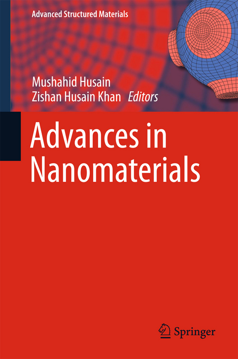
Advances in Nanomaterials (eBook)
XVIII, 429 Seiten
Springer India (Verlag)
978-81-322-2668-0 (ISBN)
Prof. Mushahid Husain is the Vice Chancellor of M.J.P. Rohilkhand University, Bareilly. Formerly, He was a Senior Professor and Director, 'Centre for Nanoscience and Nanotechnology' at Jamia Millia Islamia (Central University), New Delhi. He has been instrumental in starting M.Tech. Nanotechnology course in 2007 in Jamia Millia Islamia. Prof. Husain has completed several major research projects on amorphous semiconductors funded by various government agencies like DST, DRDO etc. He has been Vice Chairman of Semiconductor Society of India for two consecutive terms (1999 to 2003). He is also holding various positions in different academic societies. In addition, he also held the office of the Vice-President of Indian Physical Society during the session 1990-92. At present, he is the President of Society for Nano Science and Technology and secretary of one of the prestigious 'Society for Semiconductor Devices'. He has made about 27 foreign visits including University of Cambridge - UK, University of Southampton - UK, University of Princeton, New Jersey, ICTP, Italy. UNAM-Mexico, SIRIM-Malaysia, National University-Singapore, National Tsing Hua University, Hsinchu, Taiwan, US Naval Research Lab. Washington and University of Arkansas, Fayetteville where he had delivered lectures. He has delivered 111 Invited Talks at National and International Forums. A number of popular talks on All India Radio and the National TV Channel (Doordarshan) have also been presented by him. Prof. Husain has about 182 Research Papers in reputed International Journals to his credit. He has produced 36 Ph.Ds. He has also edited one book on 'Advances in Physics of Materials.' r-latin;mso-bidi-font-family:"Times New Roman"; mso-bidi-theme-font:minor-bidi;mso-ansi-language:EN-US;mso-fareast-language: EN-US;mso-bidi-language:AR-SA'>Zishan Husain Khan is working as Associate Professor (Applied Physics) in the Department of Applied Sciences & Humanities, Faculty of Engineering & Technology, Jamia Millia Islamia, New Delhi-110025 (India). He specializes in nanotechnology with special emphasis of carbon nanotubes, semiconducting nanostructures and nano-chalcogenides. His work on the fabrication of a FET based on an individual carbon nanotube using e-beam lithography and its I-V characteristics was significant. He also studied the electrical transport properties and field emission properties of bulk carbon nanotubes. Dr. Khan has also contributed significantly in the field of oxide semiconductors and synthesized ZnO nanostructures for various applications. His contribution in the field of carbon nanotubes based sensors is notable. His recent work on OLEDs based on organic semiconductors and nano-memory devices based on nanochalcogenides is expected to have significant impact on emerging field of nanotechnology. Dr Khan has earned his Ph.D. on Amorphous Semiconductors from Jamia Millia Islmia, New Delhi-110025 (India) in 1996. He joined as a post-doctoral researcher at the Center of Nanoscience and Nanotechnology, National Tsing Hua University (NTHU), Hsinchu, Taiwan in Dec. 2001 and continued there up to Feb. 2005. While pursuing his Post-Doc, Dr. Khan worked extensively on different types of nanostructures with special focus of carbon nanotubes. He has published around 84 research papers in outstanding and high impact factor journals and made over 40 presentations in conferences and symposia, which includes invited talks in the conferences. Dr. Khan has been one of founder members of Center of Nanotechnology, King Abdulaziz University, Jeddah (Suadi Arabia). He has been the guest editor of International Journal of Nanoparticles (UK), International Journal of Nano-Biomaterials (UK), International Journal of Nanomanufacturing (UK), Journal of Nanomaterials (USA), Advanced Science Letters (USA). He is also a regular reviewer of many reputed International journals.
This book provides a review of the latest research findings and key applications in the field of nanomaterials. The book contains twelve chapters on different aspects of nanomaterials. It begins with key fundamental concepts to aid readers new to the discipline of nanomaterials, and then moves to the different types of nanomaterials studied. The book includes chapters based on the applications of nanomaterials for nano-biotechnology and solar energy. Overall, the book comprises chapters on a variety of topics on nanomaterials from expert authors across the globe. This book will appeal to researchers and professional alike, and may also be used as a reference for courses in nanomaterials.
Prof. Mushahid Husain is the Vice Chancellor of M.J.P. Rohilkhand University, Bareilly. Formerly, He was a Senior Professor and Director, “Centre for Nanoscience and Nanotechnology” at Jamia Millia Islamia (Central University), New Delhi. He has been instrumental in starting M.Tech. Nanotechnology course in 2007 in Jamia Millia Islamia. Prof. Husain has completed several major research projects on amorphous semiconductors funded by various government agencies like DST, DRDO etc. He has been Vice Chairman of Semiconductor Society of India for two consecutive terms (1999 to 2003). He is also holding various positions in different academic societies. In addition, he also held the office of the Vice-President of Indian Physical Society during the session 1990-92. At present, he is the President of Society for Nano Science and Technology and secretary of one of the prestigious “Society for Semiconductor Devices”. He has made about 27 foreign visits including University of Cambridge – UK, University of Southampton - UK, University of Princeton, New Jersey, ICTP, Italy. UNAM-Mexico, SIRIM-Malaysia, National University-Singapore, National Tsing Hua University, Hsinchu, Taiwan, US Naval Research Lab. Washington and University of Arkansas, Fayetteville where he had delivered lectures. He has delivered 111 Invited Talks at National and International Forums. A number of popular talks on All India Radio and the National TV Channel (Doordarshan) have also been presented by him. Prof. Husain has about 182 Research Papers in reputed International Journals to his credit. He has produced 36 Ph.Ds. He has also edited one book on “Advances in Physics of Materials.” r-latin;mso-bidi-font-family:"Times New Roman"; mso-bidi-theme-font:minor-bidi;mso-ansi-language:EN-US;mso-fareast-language: EN-US;mso-bidi-language:AR-SA">Zishan Husain Khan is working as Associate Professor (Applied Physics) in the Department of Applied Sciences & Humanities, Faculty of Engineering & Technology, Jamia Millia Islamia, New Delhi-110025 (India). He specializes in nanotechnology with special emphasis of carbon nanotubes, semiconducting nanostructures and nano-chalcogenides. His work on the fabrication of a FET based on an individual carbon nanotube using e-beam lithography and its I-V characteristics was significant. He also studied the electrical transport properties and field emission properties of bulk carbon nanotubes. Dr. Khan has also contributed significantly in the field of oxide semiconductors and synthesized ZnO nanostructures for various applications. His contribution in the field of carbon nanotubes based sensors is notable. His recent work on OLEDs based on organic semiconductors and nano-memory devices based on nanochalcogenides is expected to have significant impact on emerging field of nanotechnology. Dr Khan has earned his Ph.D. on Amorphous Semiconductors from Jamia Millia Islmia, New Delhi-110025 (India) in 1996. He joined as a post-doctoral researcher at the Center of Nanoscience and Nanotechnology, National Tsing Hua University (NTHU), Hsinchu, Taiwan in Dec. 2001 and continued there up to Feb. 2005. While pursuing his Post-Doc, Dr. Khan worked extensively on different types of nanostructures with special focus of carbon nanotubes. He has published around 84 research papers in outstanding and high impact factor journals and made over 40 presentations in conferences and symposia, which includes invited talks in the conferences. Dr. Khan has been one of founder members of Center of Nanotechnology, King Abdulaziz University, Jeddah (Suadi Arabia). He has been the guest editor of International Journal of Nanoparticles (UK), International Journal of Nano-Biomaterials (UK), International Journal of Nanomanufacturing (UK), Journal of Nanomaterials (USA), Advanced Science Letters (USA). He is also a regular reviewer of many reputed International journals.
Foreword 6
Preface 8
Acknowledgments 11
Contents 13
Editors and Contributors 15
1 Introduction to Nanomaterials 19
Abstract 19
1.1 Introduction 20
1.2 Nanomaterials: A Revolution in 21st Century 21
1.2.1 Melting Point of the Material 22
1.2.2 Optical Studies 22
1.2.3 The Giant Magneto-Resistance (GMR) Effect 23
1.3 Classification of Nanomaterials 23
1.4 Types of Nanomaterials 24
1.4.1 Carbon Nanomaterials 24
1.4.1.1 Fullerenes 24
1.4.1.2 Carbon Nanotubes 26
1.4.1.3 Nanodiamond 28
1.4.1.4 Graphene 30
1.4.2 ZnO Nanostructures 31
1.5 Potential Applications of Nanomaterials 34
1.6 Toxicity of Nanomaterials 35
1.7 Concluding Remarks 36
References 37
2 Carbon Nanomaterials Based on Carbon Nanotubes (CNTs) 42
Abstract 42
2.1 Introduction 43
2.2 Fibers and Yarns (1D) 43
2.2.1 Brief Introduction 43
2.3 Fabrication Technologies 44
2.3.1 Spinning from Solutions 44
2.3.2 Spinning from Arrays 50
2.3.3 Spinning from Aerog 57
2.3.4 Spinning from Cotton-Like Precursors 61
2.3.5 Spinning with Dielectrophoresis 63
2.3.6 Twisting/Rolling of Films 68
2.3.7 Summary 71
2.4 Films, Membranes, Sheets and Papers (2D) 73
2.4.1 Brief Introduction 73
2.4.2 Fabrication Technologies 73
2.4.2.1 Wet Suspension Methods 73
2.4.2.2 Dry Methods 81
2.4.2.3 Direct Growth with CVD 83
2.5 Foams, Gels and Bulks (3D) 89
2.5.1 Brief Introduction 89
2.5.2 3D Bulks 89
2.5.3 Foams 92
2.5.4 Gels 105
2.6 Potential Applications 109
2.7 Concluding Remarks 111
Acknowledgments 112
References 112
3 The Synthesis, Properties, and Applications of Heteroatom-Doped Graphenes 119
Abstract 119
3.1 Introduction 119
3.2 Heteroatom Doping of Graphene 120
3.3 Properties of Heteroatom-Doped Graphene 122
3.4 Synthesis of Heteroatom-Doped Graphene 126
3.5 Applications of Heteroatom-Doped Graphene 133
3.6 Perspective 141
References 141
4 Chalcogenides to Nanochalcogenides Exploring Possibilities for Future R&
Abstract 150
4.1 Introduction 151
4.2 Synthesis of Chalcogenide Glasses 154
4.2.1 Preparation of Chalcogenides Thin Films 155
4.2.1.1 Physical Vapour Condensation 155
4.2.1.2 Sputtering 156
4.2.1.3 Pulsed-Laser Deposition 157
4.2.1.4 Chemical Vapour Deposition 159
4.3 Electrical, Optical and Thermal Properties 160
4.3.1 Electrical Transport Properties 160
4.3.1.1 The CFO Model 160
4.3.1.2 The Davis-Mott Model 161
4.3.1.3 The Charged Dangling Band Model 162
4.3.1.4 The QMT Model 163
4.3.1.5 Elliot’s Theory 163
4.3.1.6 Conduction in Band Tails 164
4.3.1.7 Conduction in Localized States 164
4.3.2 Optical Properties 165
4.3.2.1 Optical Absorption and Optical Gap 166
4.3.2.2 Absorption Process 166
Fundamental Absorption Process 166
Exciton Absorption 168
Free Carrier Absorption 168
Absorption Process Involving Impurities 169
4.3.2.3 Optical Constants of Thin Films 170
4.3.3 Studies on Chalcogenides Films 171
4.3.4 Studies on Nanostructures of Chalcogenides 175
4.3.5 Thermal Properties 185
4.3.5.1 Differential Scanning Calorimetric Studies 188
4.3.5.2 Theoretical Consideration of Crystallization Kinetics 189
4.3.6 Studies on Bulk Chalcogenides 191
4.3.7 Studies on Nano-chalcogenides 195
4.4 Applications of Chalcogenides 200
4.4.1 Memories Based on Phase-Change in Chalcogenide Glasses 200
4.4.2 Memories Based on Electrical Switching in Chalcogenide Glasses 200
4.5 Conclusion 205
References 206
5 Metal Oxide Nanostructures: Growth and Applications 218
Abstract 218
5.1 Introduction to Metal Oxides 219
5.1.1 Metal Oxide Nanostructures 221
5.2 Growth of Metal Oxide Nanostructures 223
5.2.1 Chemical Vapor Deposition 223
5.3 Growth of Indium Oxide Nanostructures 225
5.3.1 Effect of Growth Ambient: Tunable Growth of Nanowires, Nanotubes and Octahedrons 225
5.3.2 Effect of Growth Time: Regular to Irregular Nanostructures 228
5.3.3 Effect of Growth Pressure: Nanoflute to Nanotube 229
5.3.4 Effect of Gas Flow Dynamics: Horizontal to Vertically Aligned Nanostructures 231
5.4 Growth of Zinc Oxide Nanostructures (ZNT) 232
5.5 Growth of 3-D Indium-Zinc Oxide Nanostructures 233
5.6 Growth of Gallium Oxide Nanostructures 234
5.7 Application: Environmental Sensors 237
5.7.1 Hazardous Gas Sensors 237
5.7.2 Deep Ultraviolet (DUV) Photodetector 239
5.8 Summary 242
References 242
6 Metal Matrix Nanocomposites and Their Application in Corrosion Control 246
Abstract 246
6.1 Nanocomposites 247
6.2 Types of Nanocomposites 247
6.2.1 Ceramic-Matrix Nanocomposites (CMNCs) 247
6.2.2 Metal-Matrix Nanocomposites (MMNCs) 248
6.2.3 Polymer-Matrix Nanocomposites (PMNCs) 248
6.3 Synthesis Routes for Fabricating Metal Matrix Nanocomposites 249
6.3.1 Solid State Methods 249
6.3.2 Liquid State Methods 250
6.4 Major Applications of Metal Matrix Nanocomposites 254
6.5 Corrosion 255
6.5.1 Mechanism of Corrosion 256
6.5.2 Tafel Plots 257
6.5.3 Formulas Used in Corrosion Measurements 257
6.6 Corrosion Control by Metal Matrix Nanocomposites 258
References 260
7 Diamond Nanogrinding 262
Abstract 262
7.1 Introduction 263
7.2 Piezoelectric Nanogrinding 264
7.3 Stress Analysis in a Nanogrinding Grain 265
7.3.1 Analysis of Loaded Nanogrinding Grains 265
7.4 Fracture Dominated Wear Model 272
7.5 Nanogrinding 273
7.5.1 Nanogrinding Apparatus 273
7.5.2 Nanogrinding Procedure 273
7.5.3 Stress Analysis 276
7.6 Porous Nanogrinding Tools 279
7.6.1 Dissolution Models for Quartz in Bonding Bridges 282
7.6.2 Preparation of Bonding Bridges for Nanogrinding Wheels 285
7.6.3 X-ray Diffraction of Bonding Systems 287
7.6.4 Refractory Bonding Systems—Verification and Comparison of Dissolution Models for Quartz 288
7.6.5 Fusible Bonding Systems—Verification and Comparison of Dissolution Models for Quartz 294
7.7 Laser Dressing of Nanogrinding Tools 296
7.7.1 Experimental Procedures 298
7.7.1.1 Measurement of Dressing Temperatures 298
7.7.1.2 Orientation Imaging Microscopy 299
7.7.1.3 Nanogrinding Experiments 299
7.7.2 Experimental Results and Discussion 300
7.7.2.1 Laser Dressing Temperatures 300
7.7.2.2 Orientation Imaging Microscopy of Laser-Dressed Materials 305
7.7.2.3 Nanogrinding Experiments 307
7.8 Future Directions 310
Acknowledgements 311
References 311
8 Epitaxial GaN Layers: Low Temperature Growth Using Laser Molecular Beam Epitaxy Technique and Characterizations 313
Abstract 313
8.1 Introduction 314
8.2 Experimental Section 316
8.3 Result and Discussion 318
8.3.1 Cleaning and Nitridation of Sapphire 318
8.3.2 Growth of GaN Films on Sapphire Using Liquid Ga Target 321
8.3.3 Growth of GaN Layers on Sapphire Using Solid HVPE GaN Target 326
8.3.3.1 Effect of Growth Temperature 326
8.3.3.2 Effect of Laser Repetition Rates 329
8.4 Conclusion and Future Remarks 336
Acknowledgments 337
References 337
9 Aperiodic Silicon Nanowire Arrays: Fabrication, Light Trapping Properties and Solar Cell Applications 342
Abstract 342
9.1 Introduction 343
9.2 Large Area Fabrication of Silicon Nanowire Arrays 344
9.3 Morphology and Structure of SiNWs 346
9.4 Fabrication Mechanism 349
9.5 Light Trapping and Enhanced Optical Absorption in SiNW Arrays 352
9.5.1 SiNW Arrays on Bulk Silicon Wafer 352
9.5.2 SiNW Arrays on Silicon Thin Film on Glass Substrates 355
9.5.3 Theoretical Modelling/Simulation of ARC/Light Trapping for MA-EWCE SiNW Arrays 356
9.6 Omni-directional Light Trapping Properties 356
9.7 Solar Cells Basics and Importance of Silicon Nanowires 357
9.7.1 Solar Cells Basic Parameters 358
9.7.2 Silicon Nanowire Arrays Based Solar Cell Concept 359
9.8 Silicon Nanowire Arrays Based Photovoltaic Devices: Recent Developments 360
9.9 Problems and Challenges of Aperiodic SiNW Arrays Based Solar Cells 363
9.10 Effective Surface Passivation of SiNW Arrays Based Solar Cells 365
9.11 Solar Cells Based on a Vertically Aligned Radial Hetero p-n Junction SiNW Arrays 367
9.12 Solar Cells Based on a Vertically Aligned p-n Junction SiNW Arrays on Cheap Glass Substrates 368
9.13 Concluding Remarks and Future Perspective 370
Acknowledgments 371
References 371
10 Recent Trends of Gelatin Nanoparticles in Biomedical Applications 377
Abstract 377
10.1 Introduction 377
10.2 Chemical Structure 379
10.3 Preparation of GNPs 379
10.3.1 Desolvation Method 380
10.3.2 Coacervation 380
10.3.3 Solvent Evaporation Method 380
10.3.4 Spontaneous Emulsification/Solvent Diffusion Method 381
10.3.5 Nanoprecipitation Method 381
10.3.6 Salting Out Method 382
10.4 Crosslinking with GNPs 382
10.5 Characterization 383
10.6 Applications of GNPs 383
10.6.1 GNPs for Drug Delivery for Cancer and Infectious Diseases 384
10.6.2 GNPs for Protein and Vaccine Delivery 385
10.6.3 GNPs for Gene Delivery 386
10.6.4 GNPs for Ocular Drug Delivery 387
10.6.5 GNPs for Pulmonary Drug Delivery 387
10.6.6 GNPs for Nutraceutical Delivery 388
10.6.7 GNPs for Enzyme Immobilization 388
10.7 Tissue Engineering 389
10.8 Conclusions 390
References 391
11 Deployment of New Carbon Nanostructure: Graphene for Drug Delivery and Biomedical Applications 394
Abstract 394
11.1 Introduction 394
11.2 Synthesis of Graphene 396
11.3 Functionalization of Graphene Sheets 396
11.4 Applications of Graphene Sheet 399
11.4.1 Graphene in Drug Delivery: Amine-Functionalized Graphene for the Delivery of Amphotericin B for the Treatment of Visceral Leishmaniasis: In Vivo and in Vitro Studies 399
11.5 Biomedical Application of Graphene 400
11.5.1 Immobilization of Beta-Galactosidase onto Functionalized Graphene Nano-sheets for Analytical Applications 400
11.5.2 Functionalized Graphene Sheets for the Immobilization of Pharmaceutically Important Enzyme, ?-Amylase 403
11.6 Conclusions 404
Acknowledgments 405
References 405
12 Optical Coherence Tomography as Glucose Sensor in Blood 407
Abstract 407
12.1 Introduction 408
12.2 OCT's Basic Principle: Mechanism of Time Domain OCT 409
12.3 Glucose Levels in Blood 410
12.4 Application of OCT for Glucose Monitoring 410
12.5 SS-OCT in Glucose Sensing 411
12.6 Glucose Quantification in Stagnant Blood 411
12.6.1 Samples Preparation 411
12.6.2 Measurement System 412
12.6.3 Signal Processing and Results 413
12.6.4 Discussions 418
12.7 Microscopic Images for Qualitative Monitoring 420
12.7.1 Materials and Methods 420
12.7.2 Results and Discussions 421
12.8 Flow Phantom Measurements 423
12.8.1 Samples Preparation 424
12.8.2 Measurements and Signal Processing 424
12.8.3 Results and Discussion 427
12.9 In Vivo Blood Glucose Quantification 429
12.9.1 The Dorsal Skinfold Mouse Window Chamber Model 429
12.9.2 Animal Model 431
12.9.3 OCT Imaging System 431
12.9.4 Speckle Variance OCT: Blood Vessel Images 431
12.9.5 Results and Discussions 432
Acknowledgments 435
References 435
Author Index 439
| Erscheint lt. Verlag | 15.3.2016 |
|---|---|
| Reihe/Serie | Advanced Structured Materials | Advanced Structured Materials |
| Zusatzinfo | XVIII, 429 p. 246 illus., 125 illus. in color. |
| Verlagsort | New Delhi |
| Sprache | englisch |
| Themenwelt | Technik ► Elektrotechnik / Energietechnik |
| Technik ► Maschinenbau | |
| Schlagworte | Graphene • Metal Matrix Nanocomposite • Nanobiomaterials • Nanochalcogenides • Nanocomposite • nanomaterials |
| ISBN-10 | 81-322-2668-2 / 8132226682 |
| ISBN-13 | 978-81-322-2668-0 / 9788132226680 |
| Haben Sie eine Frage zum Produkt? |
Größe: 18,0 MB
DRM: Digitales Wasserzeichen
Dieses eBook enthält ein digitales Wasserzeichen und ist damit für Sie personalisiert. Bei einer missbräuchlichen Weitergabe des eBooks an Dritte ist eine Rückverfolgung an die Quelle möglich.
Dateiformat: PDF (Portable Document Format)
Mit einem festen Seitenlayout eignet sich die PDF besonders für Fachbücher mit Spalten, Tabellen und Abbildungen. Eine PDF kann auf fast allen Geräten angezeigt werden, ist aber für kleine Displays (Smartphone, eReader) nur eingeschränkt geeignet.
Systemvoraussetzungen:
PC/Mac: Mit einem PC oder Mac können Sie dieses eBook lesen. Sie benötigen dafür einen PDF-Viewer - z.B. den Adobe Reader oder Adobe Digital Editions.
eReader: Dieses eBook kann mit (fast) allen eBook-Readern gelesen werden. Mit dem amazon-Kindle ist es aber nicht kompatibel.
Smartphone/Tablet: Egal ob Apple oder Android, dieses eBook können Sie lesen. Sie benötigen dafür einen PDF-Viewer - z.B. die kostenlose Adobe Digital Editions-App.
Zusätzliches Feature: Online Lesen
Dieses eBook können Sie zusätzlich zum Download auch online im Webbrowser lesen.
Buying eBooks from abroad
For tax law reasons we can sell eBooks just within Germany and Switzerland. Regrettably we cannot fulfill eBook-orders from other countries.
aus dem Bereich


