Silicon Analog Components (eBook)
XLI, 607 Seiten
Springer New York (Verlag)
978-1-4939-2751-7 (ISBN)
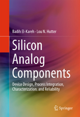
This book covers modern analog components, their characteristics, and interactions with process parameters. It serves as a comprehensive guide, addressing both the theoretical and practical aspects of modern silicon devices and the relationship between their electrical properties and processing conditions. Based on the authors' extensive experience in the development of analog devices, this book is intended for engineers and scientists in semiconductor research, development and manufacturing. The problems at the end of each chapter and the numerous charts, figures and tables also make it appropriate for use as a text in graduate and advanced undergraduate courses in electrical engineering and materials science.
Dr. Badih El-Kareh is an independent consultant, retired IBM and Texas Instruments physicist. He has over 40 years' experience in semiconductor device design, process integration, and characterization. This includes the development of advanced CMOS and BiCMOS processes and devices for analog, memory, digital, and high-voltage applications. He has 30 years' experience in academic and industrial teaching and is author of a book on VLSI Silicon Devices, a book on Modern Semiconductor Processing Technologies, and a book on Silicon Devices and Process Integration. He authored and co-authored 35 papers and has 49 US patents issued. Dr. El-Kareh is a senior member of the IEEE.
Lou Hutter has almost 35 years of experience in the semiconductor industry. As Director of the Mixed-Signal Technology Development group at TI, he was responsible for all analog, mixed-signal, RF, and power technology development in the company, supporting every major business unit. After retiring from TI in 2007, he became the General Manager of the Analog Foundry business unit at Dongbu HiTek, a S. Korean foundry, where he was a Senior VP. He was elected a TI Fellow in 1995, holds 47 U.S. patents, and has co-authored over 30 papers. His focus areas have been in high-performance analog CMOS, high-power BCD technology, power metallization, SiGe BiCMOS, technology road-mapping, and technology development methodology.
This book covers modern analog components, their characteristics, and interactions with process parameters. It serves as a comprehensive guide, addressing both the theoretical and practical aspects of modern silicon devices and the relationship between their electrical properties and processing conditions. Based on the authors' extensive experience in the development of analog devices, this book is intended for engineers and scientists in semiconductor research, development and manufacturing. The problems at the end of each chapter and the numerous charts, figures and tables also make it appropriate for use as a text in graduate and advanced undergraduate courses in electrical engineering and materials science.
Dr. Badih El-Kareh is an independent consultant, retired IBM and Texas Instruments physicist. He has over 40 years’ experience in semiconductor device design, process integration, and characterization. This includes the development of advanced CMOS and BiCMOS processes and devices for analog, memory, digital, and high-voltage applications. He has 30 years’ experience in academic and industrial teaching and is author of a book on VLSI Silicon Devices, a book on Modern Semiconductor Processing Technologies, and a book on Silicon Devices and Process Integration. He authored and co-authored 35 papers and has 49 US patents issued. Dr. El-Kareh is a senior member of the IEEE.Lou Hutter has almost 35 years of experience in the semiconductor industry. As Director of the Mixed-Signal Technology Development group at TI, he was responsible for all analog, mixed-signal, RF, and power technology development in the company, supporting every major business unit. After retiring from TI in 2007, he became the General Manager of the Analog Foundry business unit at Dongbu HiTek, a S. Korean foundry, where he was a Senior VP. He was elected a TI Fellow in 1995, holds 47 U.S. patents, and has co-authored over 30 papers. His focus areas have been in high-performance analog CMOS, high-power BCD technology, power metallization, SiGe BiCMOS, technology road-mapping, and technology development methodology.
Foreword 6
Preface 8
Acknowledgments 10
Contents 11
Abbreviations and Acronyms 18
Symbols 23
1 The World Is Analog 38
Abstract 38
1.1 Introduction 38
1.2 What's Different About Analog 40
1.2.1 Digital Design Considerations 40
1.2.2 Analog Design Considerations 42
1.2.3 Analog Technology and Manufacturing Considerations 45
1.2.3.1 Role of Bipolar Transistors in Analog Technology 49
1.3 Integration or Not 49
1.4 Analog Process Technologies 51
1.4.1 Mixed-Signal CMOS Technology 51
1.4.2 RF CMOS Technology 53
1.4.3 High-Speed BiCMOS 53
1.4.4 Analog CMOS Technology 54
1.4.4.1 Bipolar-CMOS-DMOS (BCD) Technology 56
1.4.5 Nonvolatile Memory 57
1.5 Analog Technology Roadmaps 58
References 59
2 Review of Single-Crystal Silicon Properties 62
Abstract 62
2.1 Introduction 62
2.2 Crystal Structure 62
2.3 Energy-Gap and Intrinsic Carrier Concentration 64
2.3.1 Energy Band Model 65
2.3.2 The Boltzmann Distribution 67
2.3.3 Fermi--Dirac Distribution and Density of States 68
2.4 Doping 71
2.4.1 Dopants from the Fifth Column---Donors 71
2.4.2 Dopants from the Third Column---Acceptors 72
2.4.3 Band Model for Impurities in Silicon 74
2.5 Carrier Transport 77
2.5.1 Carrier Transport by Drift---Low Field 78
2.5.2 Carrier Transport by Drift---High Field 85
2.5.3 Carrier Transport by Diffusion 87
2.5.4 Total Drift and Diffusion Current Density 88
2.5.5 Non-uniform Doping Concentration 89
2.5.6 Einstein Relation 90
2.6 Non-equilibrium Conditions 91
2.6.1 Carrier Lifetime 91
Problems 98
References 99
3 PN Junctions 101
Abstract 101
3.1 Introduction 101
3.2 Structure and Types 101
3.2.1 Cylindrical and Spherical Approximations 105
3.3 Junction Characteristics at Thermal Equilibrium 105
3.3.1 Step Junction 106
3.4 Forward-Biased Junction 117
3.4.1 Effect of Series Resistances 121
3.4.2 Effect of Surface Recombination 122
3.5 Reverse-Biased Junction 124
3.5.1 Reverse Leakage Current 126
3.5.2 Impact Ionization and Avalanche Breakdown 129
3.5.3 Reverse Recovery Time 132
3.6 Applications 135
3.6.1 Zener Diode 135
3.6.2 PIN Diode 139
Problems 141
References 144
4 Rectifying and Ohmic Contacts 146
Abstract 146
4.1 Introduction 146
4.2 Rectifying Contacts, Schottky Barrier Diode 147
4.2.1 Metal--Semiconductor Barriers 147
4.2.2 Current--Voltage Characteristics 152
4.2.3 Schottky Barrier Diode Applications 166
4.3 Ohmic Contacts 169
4.3.1 Specific Contact Resistivity 170
Problems 177
References 179
5 Bipolar and Junction Field-Effect Transistors 182
Abstract 182
5.1 Introduction 182
5.2 Bipolar Junction Transistor, BJT 184
5.2.1 Idealized Structure 184
5.2.2 NPN Transistor in a CMOS Technology 192
5.2.3 PNP Transistors in CMOS Technology 215
5.2.4 Frequency Response 217
5.2.5 BJT Applications 220
5.3 Junction Field-Effect Transistor, JFET 222
5.3.1 Idealized Normally On NJFET 222
5.3.2 JFET in a CMOS Technology 231
5.3.3 JFET Applications 233
Problems 234
References 238
6 Analog/RF CMOS 240
Abstract 240
6.1 Introduction 240
6.2 Review of MOS Properties 241
6.2.1 Flatband Condition 241
6.2.2 Accumulation and Depletion 246
6.2.3 Weak and Strong Inversion 247
6.2.4 MOS C-V Technique 252
6.3 CMOS 256
6.3.1 Review of MOSFETs, Long and Wide Channel 257
6.3.2 Analog Specific MOSFETs 279
6.3.3 Small-Size Effects 286
6.4 Analog Application 298
6.4.1 Differential Amplifier 299
6.4.2 Current Mirror 299
6.4.3 Native NMOS 300
6.4.4 Buried Channel MOSFET 301
6.4.5 Depletion-Mode MOSFET 301
Problems 302
References 304
7 High-Voltage and Power Transistors 310
Abstract 310
7.1 Introduction 310
7.2 The Drift Region 312
7.3 On-State Analysis 312
7.3.1 On-Resistance, RDS(on) 313
7.3.2 Specific On-Resistance, RSP 314
7.4 Off-State Analysis 317
7.4.1 A Simple One-Dimensional Analysis of BVDSS 318
7.4.2 Reduced Surface Field, RESURF 321
7.5 Trade-Offs 327
7.5.1 Trade-Off Between RSP and BVDSS 328
7.5.2 Switching Performance, RDS(on) x QG 329
7.6 Design and Characteristics of DEMOS 333
7.6.1 Complementary DEMOS 333
7.6.2 Field-Gap DENMOS 334
7.6.3 Subthreshold Leakage Current 335
7.6.4 Asymmetric and Symmetric DEMOS 335
7.6.5 Dielectric RESURF 336
7.6.6 Key Dimensions 337
7.6.7 Specific on-Resistance Versus Breakdown Voltage 338
7.7 Design and Characteristics of LDMOS 338
7.7.1 NLDMOS Configurations 339
7.7.2 PLDMOS 341
7.7.3 Laterally Graded Channel Effects 341
7.7.4 The Superjunction Concept 343
7.7.5 Key Dimensions 345
7.7.6 SOI Devices 347
7.7.7 Trade-Off Between RSP and BVDSS 349
7.8 High-Voltage and High-Current Effects 350
7.8.1 Quasi-Saturation 350
7.8.2 Impact Ionization and Body Current 360
7.8.3 On-State Breakdown Voltage 362
7.8.4 Self-heating and Temperature Effects 363
7.9 Safe Operating Area (SOA) 368
7.9.1 Electrical SOA 369
7.9.2 Electrothermal SOA 370
7.10 Circuit Applications 371
7.10.1 Half H-Bridge Circuit 371
7.10.2 H-Bridge Motor Driver---LDMOS Reverse Recovery 373
7.10.3 DC--DC Converter---Switching Effects 376
7.10.4 AC--DC Converter 379
Problems 381
References 384
8 Passive Components 392
Abstract 392
8.1 Introduction 392
8.2 Resistors 392
8.2.1 Definition of Terms 394
8.2.2 Polysilicon Resistor 399
8.2.3 Silicon Resistors 410
8.2.4 Thin-Film Resistors, TFR 412
8.3 Capacitors 413
8.3.1 Definition of Terms 414
8.3.2 MOS Capacitors 419
8.3.3 Poly--Insulator--Poly Capacitor, PIP 421
8.3.4 Metal--Insulator--Metal Capacitors 421
8.4 Varactors 424
8.4.1 Definition of Terms 424
8.4.2 Junction Varactors 425
8.4.3 MOS Varactors 428
8.5 Planar Spiral Inductors 432
8.5.1 Definition of Terms 432
8.6 Applications 434
8.6.1 Resistors 434
8.6.2 Capacitors 435
8.6.3 Inductors and Varactors 437
Problems 437
References 439
9 Process Integration 445
Abstract 445
9.1 Introduction 445
9.2 Analog, Mixed-Signal, and RF Components 448
9.3 Unit Processes 448
9.4 Digital CMOS 450
9.4.1 Isolation Module 451
9.4.2 Wells 453
9.4.3 Gate Stack Module 453
9.4.4 Source--Drain Module 454
9.4.5 BEOL Modules 455
9.5 MS and RF CMOS 461
9.5.1 High-Voltage CMOS 462
9.5.2 Low-Voltage Analog CMOS 462
9.5.3 Isolated NMOS 463
9.5.4 Drain-Extended CMOS 464
9.5.5 Bipolar Junction Transistors 465
9.5.6 Polysilicon and Silicon Resistors 466
9.5.7 Lateral Flux Capacitor, LFC 467
9.5.8 Vertical MIM Capacitor in Aluminum BEOL 468
9.5.9 Vertical MIM Capacitor in Copper BEOL 469
9.5.10 Inductor 471
9.6 Analog CMOS 471
9.6.1 HV Analog CMOS Transistors 471
9.6.2 Native NMOS 472
9.6.3 Depletion-Mode NMOS 472
9.6.4 Buried Channel PMOS 473
9.6.5 Junction Field-Effect Transistor 474
9.6.6 High Sheet Poly Resistor 474
9.6.7 Thin-Film Resistor 476
9.6.8 Poly--Insulator--Poly Capacitor 477
9.6.9 Buried (Subsurface) Zener Diode 479
9.7 Bipolar-CMOS-DMOS, BCD 479
9.7.1 NLDMOS 480
9.7.2 High-Frequency NLDMOS 482
9.7.3 Low-Complexity NLDMOS 483
9.7.4 Isolated-Drain NLDMOS 485
9.7.5 PLDMOS 485
Problems 486
References 488
10 Mismatch and Noise 491
Abstract 491
10.1 Introduction 491
10.2 Mismatch 491
10.2.1 Layout Configurations [3] 493
10.2.2 Inverse Area Law 495
10.2.3 MOSFET Mismatch 496
10.2.4 Bipolar Transistor Mismatch 503
10.2.5 Resistor Mismatch 505
10.2.6 Capacitor Mismatch 506
10.3 Noise 509
10.3.1 Classification of Noise 510
10.3.2 1/f Noise in CMOS 515
10.3.3 1/f Noise in Resistors 520
10.3.4 1/f Noise in Bipolar Junction Transistors, BJT 522
10.3.5 1/f Noise in Junction Field-Effect Transistors, JFET 523
10.4 Circuit Examples 524
10.4.1 Mismatch in Current Mirrors 524
10.4.2 Noise in Two-Stage Transconductance Amplifier 525
Problems 527
References 529
11 Chip Reliability 536
Abstract 536
11.1 Introduction 536
11.2 Definition of Terms and Basic Reliability Concepts 537
11.3 Reliability Models 542
11.3.1 Exponential Distribution 543
11.3.2 Normal Distribution 544
11.3.3 Lognormal Distribution 546
11.3.4 Weibull Distribution 549
11.3.5 Power Law Model 552
11.4 Failure Mechanisms 553
11.4.1 Dielectric Reliability 553
11.4.2 Electromigration and Stress Migration 565
11.4.3 Hot-Carrier Effects 574
11.4.4 Bias Temperature Instability 582
11.4.5 Joule Heating and Resistor Reliability 584
11.4.6 Plasma Charging and Damage 586
11.4.7 Latch-up 590
11.4.8 High-Voltage MOSFET Reliability 596
11.4.9 Electrostatic Discharge and Voltage Snapback 599
Problems 602
References 603
Appendix A Universal Physical Constants 615
Appendix B Properties of Silicon and GermaniumCrystals (300 K) 616
Appendix C Properties of SiO2 and Si3N4 (300 K) 619
Appendix D International System of Units 620
Appendix E The Greek Alphabet 621
Appendix F Conversion Factors 622
Index 624
| Erscheint lt. Verlag | 4.6.2015 |
|---|---|
| Zusatzinfo | XLI, 607 p. 454 illus. |
| Verlagsort | New York |
| Sprache | englisch |
| Themenwelt | Technik ► Elektrotechnik / Energietechnik |
| Technik ► Maschinenbau | |
| Schlagworte | BCD Processes and Devices • CMOS, BiCMOS Processes • Diodes, Transistors Book • El-Kareh Silicon Device Design • High-voltage DECMOS • Physics of Analog Components • Silicon Analog Components • Varactors, Capacitors Book |
| ISBN-10 | 1-4939-2751-5 / 1493927515 |
| ISBN-13 | 978-1-4939-2751-7 / 9781493927517 |
| Haben Sie eine Frage zum Produkt? |
Größe: 30,4 MB
DRM: Digitales Wasserzeichen
Dieses eBook enthält ein digitales Wasserzeichen und ist damit für Sie personalisiert. Bei einer missbräuchlichen Weitergabe des eBooks an Dritte ist eine Rückverfolgung an die Quelle möglich.
Dateiformat: PDF (Portable Document Format)
Mit einem festen Seitenlayout eignet sich die PDF besonders für Fachbücher mit Spalten, Tabellen und Abbildungen. Eine PDF kann auf fast allen Geräten angezeigt werden, ist aber für kleine Displays (Smartphone, eReader) nur eingeschränkt geeignet.
Systemvoraussetzungen:
PC/Mac: Mit einem PC oder Mac können Sie dieses eBook lesen. Sie benötigen dafür einen PDF-Viewer - z.B. den Adobe Reader oder Adobe Digital Editions.
eReader: Dieses eBook kann mit (fast) allen eBook-Readern gelesen werden. Mit dem amazon-Kindle ist es aber nicht kompatibel.
Smartphone/Tablet: Egal ob Apple oder Android, dieses eBook können Sie lesen. Sie benötigen dafür einen PDF-Viewer - z.B. die kostenlose Adobe Digital Editions-App.
Zusätzliches Feature: Online Lesen
Dieses eBook können Sie zusätzlich zum Download auch online im Webbrowser lesen.
Buying eBooks from abroad
For tax law reasons we can sell eBooks just within Germany and Switzerland. Regrettably we cannot fulfill eBook-orders from other countries.
aus dem Bereich


