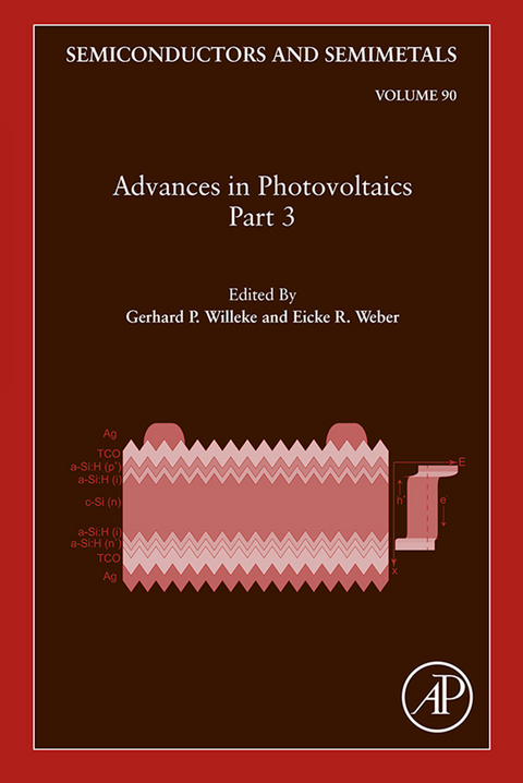
This volume is the third of a set of seven on the topic of photovoltaics. Solar cell-related technologies covered here include: ribbon silicon; heterojunction crystalline silicon; wafer equivalent crystalline silicon; and other advanced silicon solar cell structures and processes.
Semiconductors and Semimetals has distinguished itself through the careful selection of well-known authors, editors, and contributors. Originally widely known as the 'Willardson and Beer' Series, it has succeeded in publishing numerous landmark volumes and chapters. The series publishes timely, highly relevant volumes intended for long-term impact and reflecting the truly interdisciplinary nature of the field. The volumes in Semiconductors and Semimetals have been and will continue to be of great interest to physicists, chemists, materials scientists, and device engineers in academia, scientific laboratories and modern industry.
- Written and edited by internationally renowned experts
- Relevant to a wide readership: physicists, chemists, materials scientists, and device engineers in academia, scientific laboratories and modern industry
This volume is the third of a set of seven on the topic of photovoltaics. Solar cell-related technologies covered here include: ribbon silicon; heterojunction crystalline silicon; wafer equivalent crystalline silicon; and other advanced silicon solar cell structures and processes. Semiconductors and Semimetals has distinguished itself through the careful selection of well-known authors, editors, and contributors. Originally widely known as the "e;Willardson and Beer"e; Series, it has succeeded in publishing numerous landmark volumes and chapters. The series publishes timely, highly relevant volumes intended for long-term impact and reflecting the truly interdisciplinary nature of the field. The volumes in Semiconductors and Semimetals have been and will continue to be of great interest to physicists, chemists, materials scientists, and device engineers in academia, scientific laboratories and modern industry. Written and edited by internationally renowned experts Relevant to a wide readership: physicists, chemists, materials scientists, and device engineers in academia, scientific laboratories and modern industry
Front Cover 1
Advances in Photovoltaics: Part 3 4
Copyright 5
Contents 6
Contributors 8
Preface 10
Chapter One: State-of-the-Art Industrial Crystalline Silicon Solar Cells 12
1. Introduction 15
1.1. History 15
1.2. General routes for cost reduction 16
1.3. PV market today 18
1.4. Basic structure of an industrial c-Si solar cell 20
2. Operation Principle of a c-Si Solar Cell 21
2.1. Band diagram 21
2.2. Solar cell parameters 23
2.3. Fundamental efficiency limit of an ideal c-Si solar cell 24
2.4. Two-diode model 25
2.5. Radiative recombination 25
2.6. Auger recombination 26
2.7. SRH recombination 27
2.8. Surface recombination 28
2.9. Recombination and saturation current density 29
2.10. Optical losses 29
3. The Basic Firing Through SiNx:H Process 30
3.1. Wafer washing, texturization, and cleaning 31
3.2. Phosphorus diffusion 33
3.2.1. Phosphorus diffusion gettering of impurities 35
3.3. Edge isolation 36
3.4. SiNx:H deposition 36
3.5. Metallization via screen-printing 38
3.5.1. Front side metallization 39
3.5.2. Rear side metallization 40
3.5.3. Co-firing step 43
3.6. Solar cell characterization 44
4. Recent Developments on Solar Cell Front Side 45
4.1. Wafer sawing 45
4.2. Alkaline wafer texturing 46
4.3. Front contact metallization 46
4.3.1. Double print 47
4.3.2. Dual print 47
4.3.3. Stencil printing 47
4.3.4. Dispensing 48
4.3.5. Paste development 49
4.3.6. Seed-and-plate 49
4.3.7. Multi-busbar approaches 50
5. Advanced Emitter Formation 51
5.1. Improvement of homogeneous emitters 52
5.2. Selective emitters 53
5.2.1. Doped Si inks 55
5.2.2. Oxide mask process 55
5.2.3. Ion implantation process 55
5.2.4. Etch-back process 56
5.2.5. Laser doping via P-glass 59
5.2.6. Laser doping via laser chemical processing and NiAg light-induced plating 59
5.2.7. Laser doping and plating 59
5.2.8. Effect of encapsulation on blue response 60
5.2.9. Efficiency potential of selective emitters 61
6. Industrial PERC-Type Solar Cells 62
6.1. Dielectric rear side passivation 63
6.1.1. Al2O3 layers 64
6.1.2. Al2O3/SiNx:H stacks 64
6.1.3. SiO2/SiNx:H stacks 65
6.2. Formation of local rear contacts 65
6.2.1. Laser fired contacts 65
6.2.2. Etching paste 66
6.2.3. Laser ablation 66
6.2.4. Contact patterns and void formation 66
6.2.5. Interconnection issues 67
6.3. Boron-oxygen related degradation 68
6.3.1. Strategies to deal with B-O related degradation 68
6.3.2. Regeneration of B-O related defects 69
6.4. State-of-the-art industrial PERC solar cells 70
7. Summary and Outlook 71
Acknowledgments 73
References 73
Chapter Two: Amorphous Silicon/Crystalline Silicon Heterojunction Solar Cells 84
1. Introduction 85
2. Passivating c-Si Surfaces with a-Si:H 87
2.1. Recombination at surfaces 89
2.2. Physics of passivation 90
2.3. Deposition of high-quality a-Si:H films 90
2.4. Surface passivation on n- and p-type wafers 93
3. From Passivated Wafers to Complete Solar Cells 94
3.1. Wafer cleaning and texturing 94
3.2. Electron and hole collectors: Doped a-Si:H layers 96
3.3. Transparent conductive oxide layers 97
3.4. Metallization 101
3.5. Record cells 103
4. Losses in Silicon Heterojunction Solar Cells 106
4.1. Voc losses 106
4.2. FF losses 106
4.3. Jsc losses 107
5. Industrialization and Commercialization 110
5.1. General status 110
5.2. Material requirements 111
5.3. Temperature coefficient and energy yield 113
5.4. Metallization 114
5.5. Tools and production technologies 114
5.5.1. Wet chemistry 115
5.5.2. a-Si:H layer deposition 115
5.5.3. Front and rear TCO, and rear metallization 116
5.5.4. Final processing 117
5.6. Production costs 118
6. Future Directions and Outlook 119
Acknowledgments 121
References 121
Chapter Three: Overview of Thin-Film Solar Cell Technologies 132
1. Introduction 132
2. Market Shares of TF in PV 134
3. TF Device Efficiencies in Laboratory and Industry 136
4. Future Developments of TF Technologies in PV 139
References 147
Index 148
Contents of Volumes in this Series 152
Amorphous Silicon/Crystalline Silicon Heterojunction Solar Cells
Christophe Ballif*,1; Stefaan De Wolf*; Antoine Descoeudres*; Zachary C. Holman† * Photovoltaics and Thin-Film Electronics Laboratory, Institute of Microengineering (IMT), Ecole Polytechnique Fédérale de Lausanne (EPFL), Neuchâtel, Switzerland
† School of Electrical, Computer, and Energy Engineering, Arizona State University, Tempe, Arizona, USA
1 Corresponding author: email address: christophe.ballif@epfl.ch
Abstract
Silicon heterojunction solar cells are crystalline silicon-based devices in which thin amorphous silicon layers deposited on the wafer surfaces serve as passivated, carrier-selective contacts. The success of this technology is attributable to the ability of amorphous silicon to passivate dangling bonds—thereby removing surface recombination sites—without blocking charge carrier transport. This unique combination allows the recombination-active metal contacts to be displaced from the wafer surfaces, enabling record-high open-circuit voltages of up to 750 mV and efficiencies of up to 25.6%. This chapter introduces the silicon heterojunction concept and discusses device fabrication, operation, and manufacturing. Active areas of research and likely future developments are identified throughout.
Keywords
Silicon
Heterojunction
Solar cell
Photovoltaics
Amorphous silicon
Transparent conductive oxide
1 Introduction
Silicon wafer-based solar cells have dominated the photovoltaics market for decades and may well continue to do so for years to come. Several key factors explain the success of this technology: Silicon is a well-studied semiconductor with known optoelectronic properties; it is abundant and nontoxic, and the price of multicrystalline silicon has witnessed an unprecedented drop in the last few years, partially because of a temporary production overcapacity, especially in Asia; and silicon solar cell technology has greatly benefited from the accumulated knowledge in semiconductor processing developed by the microelectronics community. An important strength of the current industrial silicon solar cell technology is its fabrication simplicity. Only a few steps suffice to fabricate a full device, where each step often fulfills several roles. Examples of this are the emitter diffusion process, which simultaneously getters impurities from the bulk of the wafer, and the metal contact firing through the silicon nitride anti-reflection coating, during which bulk hydrogenation of the wafer also occurs. A drawback of this simplicity is that further improvements in device performance must rely on the increasing sophistication of existing processes, while fundamental shortcomings of the technology are hard to overcome. One such critical limitation is carrier recombination at the electrical contacts.
Carrier recombination in silicon is a well-understood phenomenon and its minimization is a key factor in obtaining high-efficiency solar cells. We make a distinction between intrinsic recombination (Auger and band-to-band radiative recombination) and deep-defect-mediated recombination (Richter et al., 2013). Importantly, the latter type of recombination can in theory be completely eliminated by using perfect crystals, combined with an “ideal” solar cell architecture. This structure should feature perfectly passivated surfaces and contacts. Taking a 100-μm-thick wafer, such a solar cell would yield an open-circuit voltage (Voc) of about 770 mV (Richter et al., 2013; Tiedje et al., 1984). Note that, with perfect contacts, the Voc represents the energetic distance between the quasi-Fermi levels, which themselves express the density of excess charge carriers present in the material as a consequence of shining light on it. An important reason why the Voc can never equal the bandgap of the absorber—1.12 eV for crystalline silicon (c-Si) at room temperature—is not only the operating temperature of the device but also the aforementioned intrinsic recombination losses. Despite this, it is possible to come close to the 770 mV limit in real devices with excellent surface and contact passivation.
Defect recombination in the bulk of c-Si has been successfully combated in recent decades, as evidenced by the ever-increasing quality of silicon wafers on the market. Surface passivation has also improved: A number of dielectric passivation layers are available that can passivate p-type and n-type surfaces very well. These include materials like silicon oxides (Benick et al., 2011; Deal and Grove, 1965; Green, 2009; Schultz et al., 2004; Zhao et al., 1998), amorphous silicon nitrides (Lanford and Rand, 1978; Lauinger et al., 1996) and aluminum oxide (Agostinelli et al., 2006; Hezel and Jaeger, 1989; Hoex et al., 2006). Surface passivation can be accomplished in two fundamentally different ways: Either the surface defect states are removed, or the excess charge carriers are screened from the surface defects by an internal electrical field. The former is known as chemical surface passivation and can be obtained by, e.g., hydrogenation of these defects. The latter is known as field-effect passivation and is usually obtained by deposition of a fixed-charge dielectric on the surface under study, thereby repelling minority carriers inside the wafer from the defective surfaces. Positive-fixed-charge dielectrics repel the positively charged holes inside the semiconductor from the surfaces, and are ideally suited to passivate n-type surfaces. A prime example is silicon nitride, which has been used for the passivation of phosphorus-doped emitters in homojunction technology (Lanford and Rand, 1978; Lauinger et al., 1996). Negative-fixed-charge dielectrics repel negatively charged electrons from the surfaces and are used to passivate p-type surfaces. Here, the most studied dielectric is aluminum oxide, which is a material that received significant attention in the last few years as a potential passivating layer for the rear surface of homojunction solar cells (Agostinelli et al., 2006; Hezel and Jaeger, 1989; Hoex et al., 2006). Silicon nitride layers can be relatively easily integrated into existing c-Si solar cell processing, whereas the successful integration of aluminum oxide layers into industrial solar cells has proven to be more of a challenge.
In all cases, contacts are needed to extract carriers from the solar cell. In standard homojunction solar cell technology, where the junction is fabricated by thermal diffusion or ion implantation, these contacts are usually defined by locally opening the dielectric passivating layers and making a direct Ohmic contact between the metal and semiconductor. Whereas the contact resistances of such contacts can be made low, the minority-carrier recombination occurring at their surfaces is of significant concern. This issue is fundamentally resolved by silicon heterojunction technology, where a thin, wider-bandgap layer is inserted between the metal contact and the optically active absorber (i.e., the silicon wafer). Qualitatively, this type of contact can be considered as a semi-permeable membrane for carrier extraction. On the one hand, it should prevent generated carriers from being collected instantaneously, as this will lower the energetic splitting of the quasi-Fermi levels and thus reduce the voltage of the device. On the other hand, the contacts should be sufficiently electronically transparent to guarantee that carriers can be collected at the device terminals before they recombine in the wafer due to intrinsic recombination processes. In principle, such contacts can be fabricated in several ways. Irrespective of the materials used, passivated contacts should feature excellent (chemical) surface passivation while also giving charge carriers an incentive to be driven toward either the electron- or the hole-collecting layers. In this chapter, the focus will be on heterojunction solar cells with layers fabricated from thin films of amorphous silicon or related materials.
2 Passivating c-Si Surfaces with a-Si:H
For silicon wafer-based devices, thin films of hydrogenated amorphous silicon (a-Si:H) are particularly appealing candidates for passivated-contact formation. First, a-Si:H passivates c-Si surfaces very well, with electrical properties that are on par with the best dielectrics available. The passivation is mostly chemical, principally due to hydrogenation of surface states. Second, such layers can be doped relatively well, either n- or p-type, by adding the appropriate process gasses during deposition. This property enables the fabrication of contacts that are selective for either electron collection (when n-type a-Si:H is used), or hole collection (when p-type a-Si:H is used). This is of significant utility, as it allows us to not simply make passivating contacts but also to escape the need for a homojunction in the wafer. As the lateral conductivity of the a-Si:H layers is quite low, transparent electrodes that serve electrical and optical roles are usually applied. Another important reason for the success of such layers is the available knowledge regarding thin-film deposition technology. Whereas silicon homojunction solar cell technology has benefited greatly from developments taking place within...
| Erscheint lt. Verlag | 1.12.2014 |
|---|---|
| Sprache | englisch |
| Themenwelt | Technik ► Elektrotechnik / Energietechnik |
| Technik ► Maschinenbau | |
| ISBN-10 | 0-12-388418-7 / 0123884187 |
| ISBN-13 | 978-0-12-388418-3 / 9780123884183 |
| Haben Sie eine Frage zum Produkt? |
Größe: 5,6 MB
Kopierschutz: Adobe-DRM
Adobe-DRM ist ein Kopierschutz, der das eBook vor Mißbrauch schützen soll. Dabei wird das eBook bereits beim Download auf Ihre persönliche Adobe-ID autorisiert. Lesen können Sie das eBook dann nur auf den Geräten, welche ebenfalls auf Ihre Adobe-ID registriert sind.
Details zum Adobe-DRM
Dateiformat: PDF (Portable Document Format)
Mit einem festen Seitenlayout eignet sich die PDF besonders für Fachbücher mit Spalten, Tabellen und Abbildungen. Eine PDF kann auf fast allen Geräten angezeigt werden, ist aber für kleine Displays (Smartphone, eReader) nur eingeschränkt geeignet.
Systemvoraussetzungen:
PC/Mac: Mit einem PC oder Mac können Sie dieses eBook lesen. Sie benötigen eine
eReader: Dieses eBook kann mit (fast) allen eBook-Readern gelesen werden. Mit dem amazon-Kindle ist es aber nicht kompatibel.
Smartphone/Tablet: Egal ob Apple oder Android, dieses eBook können Sie lesen. Sie benötigen eine
Geräteliste und zusätzliche Hinweise
Buying eBooks from abroad
For tax law reasons we can sell eBooks just within Germany and Switzerland. Regrettably we cannot fulfill eBook-orders from other countries.
Größe: 16,7 MB
Kopierschutz: Adobe-DRM
Adobe-DRM ist ein Kopierschutz, der das eBook vor Mißbrauch schützen soll. Dabei wird das eBook bereits beim Download auf Ihre persönliche Adobe-ID autorisiert. Lesen können Sie das eBook dann nur auf den Geräten, welche ebenfalls auf Ihre Adobe-ID registriert sind.
Details zum Adobe-DRM
Dateiformat: EPUB (Electronic Publication)
EPUB ist ein offener Standard für eBooks und eignet sich besonders zur Darstellung von Belletristik und Sachbüchern. Der Fließtext wird dynamisch an die Display- und Schriftgröße angepasst. Auch für mobile Lesegeräte ist EPUB daher gut geeignet.
Systemvoraussetzungen:
PC/Mac: Mit einem PC oder Mac können Sie dieses eBook lesen. Sie benötigen eine
eReader: Dieses eBook kann mit (fast) allen eBook-Readern gelesen werden. Mit dem amazon-Kindle ist es aber nicht kompatibel.
Smartphone/Tablet: Egal ob Apple oder Android, dieses eBook können Sie lesen. Sie benötigen eine
Geräteliste und zusätzliche Hinweise
Buying eBooks from abroad
For tax law reasons we can sell eBooks just within Germany and Switzerland. Regrettably we cannot fulfill eBook-orders from other countries.
aus dem Bereich


