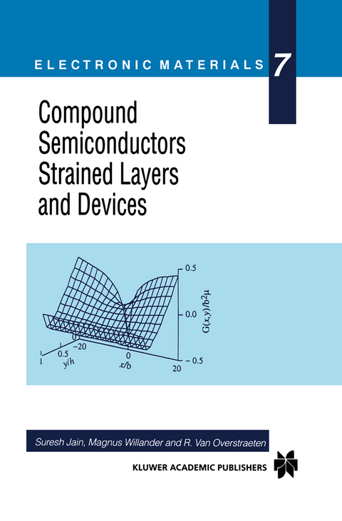
Compound Semiconductors Strained Layers and Devices
Springer-Verlag New York Inc.
978-1-4613-7000-0 (ISBN)
It is due to the strain mediated band-structure engineering that mid-IR lasers with good per- formance have been fabricated in several laboratories around the world. Many devices based on strained layers have reached the market place. This book de- scribes recent work on the growth, characterization and properties o(compound semiconductors strained layers and devices fabricated using them.
1 Introduction.- 1.1 Evolution of strained layers.- 1.2 Conventional III-V-based heterostructures.- 1.3 III-Nitrides.- 1.4 Wide bandgap II-VI semiconductors.- 1.5 Material parameters.- 1.6 Scope and organization of this book.- 2 Characterization and growth.- 2.1 Methods of characterization.- 2.2 Epitaxial growth methods.- 2.3 Growth of conventional III-V semiconductors.- 2.4 Growth of II-VI semiconductors.- 2.5 Growth of Ill-nitride epilayers.- 3 Strain and critical thickness.- 3.1 Strain and energies of epilayers.- 3.2 Processes involved in dislocation generation.- 3.3 Critical thickness.- 4 Strain relaxation and defects.- 4.1 Strain in GeSi layers.- 4.2 Strain in III-V semiconductor layers.- 4.3 Strain in II-VI layers.- 4.4 Strain and defects in Ill-Nitride layers.- 5 Band structure and optical properties.- 5.1 Band structure.- 5.2 Band offsets.- 5.3 Optical properties of III-V semiconductors.- 5.4 Optical properties of II-VI semiconductors.- 5.5 Optical properties of Ill-Nitrides.- 6 Electrical and magnetic properties.- 6.1 Electrical properties of II-VI semiconductors.- 6.2 Electrical properties of n-type GaN.- 6.3 Electrical properties of p-type Ill-Nitrides.- 6.4 Electrical properties A1N, InN and alloys.- 6.5 Schottky barriers and ohmic contacts.- 6.6 Effect of applied electric field.- 6.7 Piezoelectric effect.- 6.8 Effect of magnetic field on semiconductors.- 7 Strained layer optoelectronic devices.- 7.1 Conventional-Ill-V semiconductor lasers.- 7.2 ZnSe-based light emitters and other devices.- 7.3 Other II-VI semiconductor applications.- 7.4 Ill-Nitride Light Emitting Diodes.- 7.5 GaN based Lasers.- 8 Transistors.- 8.1 InGaAs transistors.- 8.2 II-VI semiconductor transistors.- 8.3 Ill-Nitride based transistors.- 8.4 Device Processing.- 9 Summary and conclusions.- 9.1 Growth, defects and strain.- 9.2 Band structure and electronic properties.- 9.3 Applications and future work.- Appendix A.
| Reihe/Serie | Electronic Materials Series ; 7 |
|---|---|
| Zusatzinfo | 8 Illustrations, black and white; XII, 337 p. 8 illus. |
| Verlagsort | New York, NY |
| Sprache | englisch |
| Maße | 155 x 235 mm |
| Themenwelt | Technik ► Elektrotechnik / Energietechnik |
| Technik ► Maschinenbau | |
| ISBN-10 | 1-4613-7000-0 / 1461370000 |
| ISBN-13 | 978-1-4613-7000-0 / 9781461370000 |
| Zustand | Neuware |
| Haben Sie eine Frage zum Produkt? |
aus dem Bereich


