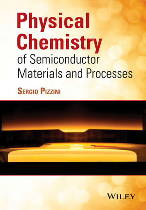
Physical Chemistry of Semiconductor Materials and Processes
John Wiley & Sons Inc (Verlag)
978-1-118-51457-3 (ISBN)
The development of solid state devices began a little more than a century ago, with the discovery of the electrical conductivity of ionic solids. Today, solid state technologies form the background of the society in which we live.
The aim of this book is threefold: to present the background physical chemistry on which the technology of semiconductor devices is based; secondly, to describe specific issues such as the role of defects on the properties of solids, and the crucial influence of surface properties; and ultimately, to look at the physics and chemistry of semiconductor growth processes, both at the bulk and thin-film level, together with some issues relating to the properties of nano-devices.
Divided into five chapters, it covers:
Thermodynamics of solids, including phases and their properties and structural order
Point defects in semiconductors
Extended defects in semiconductors and their interactions with point defects and impurities
Growth of semiconductor materials
Physical chemistry of semiconductor materials processing
With applications across all solid state technologies,the book is useful for advanced students and researchers in materials science, physics, chemistry, electrical and electronic engineering. It is also useful for those in the semiconductor industry.
SERGIO PIZZINI Department of Materials Science, University of Milano-Bicocca, Italy
Preface ix
1. Thermodynamics of Homogeneous and Heterogeneous Semiconductor Systems 1
1.1 Introduction 1
1.2 Basic Principles 2
1.3 Phases and Their Properties 7
1.3.1 Structural Order of a Phase 7
1.4 Equations of State of Thermodynamic Systems 11
1.4.1 Thermodynamic Transformations and Functions of State 11
1.4.2 Work Associated with a Transformation, Entropy and Free Energy 12
1.4.3 Chemical Potentials 14
1.4.4 Free Energy and Entropy of Spontaneous Processes 15
1.4.5 Effect of Pressure on Phase Transformations, Polymorphs/Polytypes Formation and Their Thermodynamic Stability 16
1.4.6 Electrochemical Equilibria and Electrochemical Potentials of Charged Species 21
1.5 Equilibrium Conditions of Multicomponent Systems Which Do Not React Chemically 23
1.6 Thermodynamic Modelling of Binary Phase Diagrams 28
1.6.1 Introductory Remarks 28
1.6.2 Thermodynamic Modelling of Complete and Incomplete Miscibility 29
1.6.3 Thermodynamic Modelling of Intermediate Compound Formation 40
1.6.4 Retrograde Solubility, Retrograde Melting and Spinodal Decomposition 40
1.7 Solution Thermodynamics and Structural and Physical Properties of Selected Semiconductor Systems 43
1.7.1 Introductory Remarks 43
1.7.2 Au-Ag and Au-Cu Alloys 45
1.7.3 Silicon and Germanium 49
1.7.4 Silicon-Germanium Alloys 53
1.7.5 Silicon- and Germanium-Binary Alloys with Group III and Group IV Elements 55
1.7.6 Silicon-Tin and Germanium-Tin Alloys 61
1.7.7 Carbon and Its Polymorphs 62
1.7.8 Silicon Carbide 67
1.7.9 Selenium-Tellurium Alloys 69
1.7.10 Binary and Pseudo-binary Selenides and Tellurides 71
1.7.11 Arsenides, Phosphides and Nitrides 81
1.8 Size-Dependent Properties, Quantum Size Effects and Thermodynamics of Nanomaterials 93
Appendix 98
Use of Electrochemical Measurements for the Determination of the Thermodynamic Functions of Semiconductors 98
References 103
2. Point Defects in Semiconductors 117
2.1 Introduction 117
2.2 Point Defects in Ionic Solids: Modelling the Electrical Conductivity of Ionic Solids by Point Defects-Mediated Charge Transfer 119
2.3 Point Defects and Impurities in Elemental Semiconductors 127
2.3.1 Introduction 127
2.3.2 Vacancies and Self-Interstitials in Semiconductors with the Diamond Structure: an Attempt at a Critical Discussion of Their Thermodynamic and Transport Properties 129
2.3.3 Effect of Defect–Defect Interactions on Diffusivity: Trap-and-Pairing Limited Diffusion Processes 145
2.3.4 Light Impurities in Group IV Semiconductors: Hydrogen, Carbon, Nitrogen, Oxygen and Their Reactivity 153
2.4 Defects and Non-Stoichiometry in Compound Semiconductors 167
2.4.1 Structural and Thermodynamic Properties 167
2.4.2 Defect Identification in Compound Semiconductors 171
2.4.3 Non-Stoichiometry in Compound Semiconductors 171
References 181
3. Extended Defects in Semiconductors and Their Interactions with Point Defects and Impurities 195
3.1 Introduction 195
3.2 Dislocations in Semiconductors with the Diamond Structure 196
3.2.1 Geometrical Properties 196
3.2.2 Energy of Regular Straight Dislocations 201
3.2.3 Dislocation Motion 203
3.2.4 Dislocation Reconstruction 205
3.2.5 Electronic Structure of Dislocations in Si and Ge, Theoretical Studies and Experimental Evidences 208
3.3 Dislocations in Compound Semiconductors 215
3.3.1 Electronic Structure of Dislocations in Compound Semiconductors 216
3.4 Interaction of Defects and Impurities with Extended Defects 219
3.4.1 Introduction 219
3.4.2 Thermodynamics of Defect Interactions with Extended Defects 220
3.4.3 Thermodynamics of Interaction of Neutral Defects and Impurities with EDs 221
3.4.4 Kinetics of Interaction of Point Defects, Impurities and Extended Defects: General Concepts 228
3.4.5 Kinetics of Interaction Reactions: Reaction Limited Processes 230
3.4.6 Kinetics of Interaction Reactions: Diffusion-Limited Reactions 230
3.5 Interaction of Atomic Defects with Extended Defects: Theoretical and Experimental Evidence 232
3.5.1 Interaction of Point Defects with Extended Defects 232
3.5.2 Hydrogen-Dislocation Interaction in Silicon 233
3.5.3 Interaction of Oxygen with Dislocations 235
3.6 Segregation of Impurities at Surfaces and Interfaces 236
3.6.1 Introduction 236
3.6.2 Grain Boundaries in Polycrystalline Semiconductors 236
3.6.3 Structure of Grain Boundaries and Their Physical Properties 239
3.6.4 Segregation of Impurities at Grain Boundaries and Their Influence on Physical Properties 241
3.7 3D Defects: Precipitates, Bubbles and Voids 243
3.7.1 Thermodynamic and Structural Considerations 243
3.7.2 Oxygen and Carbon Segregation in Silicon 246
3.7.3 Silicides Precipitation 249
3.7.4 Bubbles and Voids 249
References 251
4. Growth of Semiconductor Materials 265
4.1 Introduction 265
4.2 Growth of Bulk Solids by Liquid Crystallization 266
4.2.1 Growth of Single Crystal and Multicrystalline Ingots by Liquid Phase Crystallization 268
4.2.2 Growth of Single Crystals or Multicrystalline Materials by Liquid Crystallization Processes: Impact of Environmental Interactions on the Chemical Quality 274
4.2.3 Growth of Bulk Solids by Liquid Crystallization Processes: Solubility of Impurities in Semiconductors and Their Segregation 287
4.2.4 Growth of Bulk Solids by Liquid Crystallization Processes: Pick-Up of Impurities 290
4.2.5 Constitutional Supercooling 295
4.2.6 Growth Dependence of the Impurity Pick-Up and Concentration Profiling 298
4.2.7 Purification of Silicon by Smelting with Al 299
4.3 Growth of Ge-Si Alloys, SiC, GaN, GaAs, InP and CdZnTe from the Liquid Phase 300
4.3.1 Growth of Si-Ge Alloys 301
4.3.2 Growth of SiC from the Liquid Phase 303
4.3.3 Growth of GaN from the Liquid Phase 304
4.3.4 Growth of GaAs, InP, ZnSe and CdZnTe 309
4.4 Single Crystal Growth from the Vapour Phase 318
4.4.1 Generalities 318
4.4.2 Growth of Silicon, ZnSe and Silicon Carbide from the Vapour Phase 319
4.4.3 Epitaxial Growth of Single Crystalline Layers of Elemental and Compound Semiconductors 323
4.5 Growth of Poly/Micro/Nano-Crystalline Thin Film Materials 332
4.5.1 Introduction 332
4.5.2 Growth of Nanocrystalline/Microcrystalline Silicon 334
4.5.3 Growth of Silicon Nanowires 337
4.5.4 Growth of Films of CdTe and of Copper Indium (Gallium) Selenide (CIGS) 342
References 345
5. Physical Chemistry of Semiconductor Materials Processing 363
5.1 Introduction 363
5.2 Thermal Annealing Processes 364
5.2.1 Thermal Decomposition of Non-stoichiometric Amorphous Phases for Nanofabrication Processes 367
5.2.2 Other Problems of a Thermodynamic or Kinetic Nature 369
5.3 Hydrogen Passivation Processes 372
5.4 Gettering and Defect Engineering 376
5.4.1 Introduction 376
5.4.2 Thermodynamics of Gettering 377
5.4.3 Physics and Chemistry of Internal Gettering 378
5.4.4 Physics and Chemistry of External Gettering 382
5.5 Wafer Bonding 390
References 391
Index 399
| Verlagsort | New York |
|---|---|
| Sprache | englisch |
| Maße | 178 x 252 mm |
| Gewicht | 785 g |
| Themenwelt | Naturwissenschaften ► Chemie ► Physikalische Chemie |
| Naturwissenschaften ► Physik / Astronomie ► Elektrodynamik | |
| Technik ► Elektrotechnik / Energietechnik | |
| Technik ► Maschinenbau | |
| ISBN-10 | 1-118-51457-2 / 1118514572 |
| ISBN-13 | 978-1-118-51457-3 / 9781118514573 |
| Zustand | Neuware |
| Haben Sie eine Frage zum Produkt? |
aus dem Bereich


