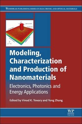
Modeling, Characterization and Production of Nanomaterials
Woodhead Publishing Ltd (Verlag)
978-1-78242-228-0 (ISBN)
- Titel erscheint in neuer Auflage
- Artikel merken
Nano-scale materials have unique electronic, optical, and chemical properties which make them attractive for a new generation of devices. Part one of Modeling, Characterization, and Production of Nanomaterials: Electronics, Photonics and Energy Applications covers modeling techniques incorporating quantum mechanical effects to simulate nanomaterials and devices, such as multiscale modeling and density functional theory. Part two describes the characterization of nanomaterials using diffraction techniques and Raman spectroscopy. Part three looks at the structure and properties of nanomaterials, including their optical properties and atomic behaviour. Part four explores nanofabrication and nanodevices, including the growth of graphene, GaN-based nanorod heterostructures and colloidal quantum dots for applications in nanophotonics and metallic nanoparticles for catalysis applications.
Professor Vinod Tewary, National Institute for Standards and Technology (NIST), USA Professor Yong Zhang, University of North Carolina, USA.
List of contributors
Woodhead Publishing Series in Electronic and Optical Materials
Part One: Modeling techniques for nanomaterials
1: Multiscale modeling of nanomaterials: recent developments and future prospects
Abstract
1.1 Introduction
1.2 Methods
1.3 Nanomaterials
1.4 Application examples
1.5 Conclusion
2: Multiscale Green’s functions for modeling of nanomaterials
Abstract
Acknowledgments
2.1 Introduction
2.2 Green’s function method: the basics
2.3 Discrete lattice model of a solid
2.4 Lattice statics Green’s function
2.5 Multiscale Green’s function
2.6 Causal Green’s function for temporal modeling
2.7 Application to 2D graphene
2.8 Conclusions and future work
3: Numerical simulation of nanoscale systems and materials
Abstract
Acknowledgments
3.1 Introduction
3.2 Molecular statics and dynamics: an overview
3.3 Static calculations of strain due to interface
3.4 Dynamic calculations of kinetic frictional properties
3.5 Fundamental properties of dynamic ripples in graphene
3.6 Conclusions and general remarks
Disclaimer
Part Two: Characterization techniques for nanomaterials
4: TEM studies of nanostructures
Abstract
Acknowledgments
4.1 Introduction
4.2 Polarity determination and stacking faults of 1D ZnO nanostructures
4.3 Structure analysis of superlattice nanowire by TEM: a case of SnO2 (ZnO:Sn)n nanowire
4.4 TEM analysis of 1D nanoheterostructure
4.5 Concluding remarks
5: Characterization of strains and defects in nanomaterials by diffraction techniques
Abstract
Acknowledgments
5.1 Introduction
5.2 Section 1: diffraction profile shift due to residual strains/stresses
5.3 Section 1: conclusions
5.4 Section 2: diffraction profile broadening due to crystalline defects and strains and their influence on ferroelectric thin films
5.5 Section 2: conclusions
6: Recent advances in thermal analysis of nanoparticles: methods, models and kinetics
Abstract
6.1 Introduction
6.2 Thermal analysis methods
6.3 Thermal analysis of nanoparticle purity and composition
6.4 Evaluation of nanoparticle-containing composites
6.5 Monitoring kinetics of thermal transitions
6.6 Trends in development of thermal analysis for nanoparticles
6.7 Conclusions
7: Raman spectroscopy and molecular simulation studies of graphitic nanomaterials
Abstract
7.1 Introduction
7.2 Literature review
7.3 Methodology
7.4 Temperature-dependent Raman spectra
7.5 Application of MD to SWCNT structural analysis
7.6 Conclusion
Part Three: Structure and properties of nanomaterials: modeling and its experimental applications
8: Carbon-based nanomaterials
Abstract
8.1 Introduction
8.2 Outline
8.3 Electronic structure of graphite
8.4 Types of CNTs
8.5 Types of nanoribbons
8.6 DOS and quantum capacitance
8.7 CNT tunnel FETs
8.8 ITRS requirements—2024
8.9 Comparison between a CNT-MOSFET and TFET
8.10 Carbon nanotube vs. graphene nanoribbon
8.11 Summary
9: Atomic behavior and structural evolution of alloy nanoparticles during thermodynamic processes
Abstract
9.1 Introduction
9.2 Simulation method
9.3 Results and discussion
9.4 Conclusions and future outlook
Part Four: Nanofabrication and nanodevices: modeling and applications
10: Metallic nanoparticles for catalysis applications
Abstract
Acknowledgments
10.1 Introduction
10.2 Synthesis of nanoalloys and preparation of nanocatalysts
10.3 Structural characterizations of nanoalloy catalysts
10.4 Applications in heterogeneous catalysis
10.5 Summary and future perspectives
11: Physical approaches to tuning luminescence process of colloidal quantum dots and applications in optoelectronic devices
Abstract
11.1 Introduction
11.2 Annealing effect on the luminescence of CQDs and WLE by single-size CQDs
11.3 Photooxidation effect on the luminescence of CQDs
11.4 Plasmonic coupling effect on the luminescence of CQDs
11.5 Microscale fluorescent color patterns realized by plasmonic coupling
11.6 CQDs applications in white LEDs
11.7 Conclusions and future trends
12: Growth of GaN-based nanorod heterostructures (core-shell) for optoelectronics and their nanocharacterization
Abstract
12.1 Introduction
12.2 MOVPE growth of InGaN/GaN core-shell heterostructures
12.3 Nanocharacterization: structure and optics
12.4 Conclusions for nitride wire-LEDs practical issues
13: Graphene photonic structures
Abstract
Acknowledgments
13.1 Introduction
13.2 Growth of 3C-SiC thin film on Si (111) using MBE
13.3 Laser-induced conversion from 3C-SiC thin film to graphene
13.4 Patterning of periodic graphene micro- or nanostructure for photonic application
13.5 Conclusions
14: Nanophotonics: From quantum confinement to collective interactions in metamaterial heterostructures
Abstract
Acknowledgments
14.1 Introduction
14.2 Atomistic modeling of low-dimensional materials: modeling collective modes with DFT
14.3 Spectral properties of multilayer structures
Disclaimer
14.4 Sources of further information
15: Plasma deposition and characterization technologies for structural and coverage optimization of materials for nanopatterned devices
Abstract
15.1 Introduction
15.2 Need for structural engineering of patterned structures
15.3 Deposition technology and source design for nanopatterned devices
15.4 Use of advanced metrology on patterned features to optimize deposition technologies and enhance performance of nanopatterned devices
15.5 Examples of optimized nanopatterned devices
15.6 Commentary on future trends
15.7 Instructive sources related to deposition technology and structural engineering of films
16: Calculation of bandgaps in nanomaterials using Harbola-Sahni and van Leeuwen-Baerends potentials
Abstracts
16.1 Introduction
16.2 Band-gap calculations in density-functional theory and derivative discontinuity of Kohn-Sham potential
16.3 Kohn-Sham potential in terms of the orbitals: exact exchange and HS potential
16.4 Calculation of bandgaps for bulk materials using the HS potential
16.5 Density-based calculations using the vLB potential
16.6 Application to clusters of graphene and hexagonal boron nitride
16.7 Discussion and concluding remarks
17: Modeling and simulation of nanomaterials in fluids: nanoparticle self-assembly
Abstract
Acknowledgments
17.1 Introduction
17.2 Experimental techniques
17.3 Modeling and analysis
17.4 Simulation methods
17.5 Statistical inference and model selection
17.6 Direct study of nanofluids
17.7 Conclusion and future trends
17.8 Sources of further information
18: Atomistic modeling of nanostructured materials for novel energy application
Abstract
18.1 Introduction
18.2 Overview of computational methods
18.3 Selected topics of modeling nanomaterials for energy nanotechnology
18.4 Summary and perspective
19: The mechanical and electronic properties of two-dimensional superlattices
Abstract
Acknowledgments
19.1 Introduction
19.2 Synthesis of 2D hybrid-domain superlattices
19.3 Mechanical properties of heterostructures
19.4 Electronic properties of hybrid-domain superlattices
19.5 Perspectives and concluding remarks
20: Nanostructured two-dimensional materials
Abstract
Acknowledgments
20.1 Layered two-dimensional semiconductors as competitive rivals of graphene
20.2 Improvement of fabrication methods for 2D semiconductors
20.3 Future trends
Index
| Reihe/Serie | Woodhead Publishing Series in Electronic and Optical Materials |
|---|---|
| Verlagsort | Cambridge |
| Sprache | englisch |
| Maße | 152 x 229 mm |
| Gewicht | 950 g |
| Themenwelt | Technik |
| ISBN-10 | 1-78242-228-5 / 1782422285 |
| ISBN-13 | 978-1-78242-228-0 / 9781782422280 |
| Zustand | Neuware |
| Haben Sie eine Frage zum Produkt? |
aus dem Bereich


