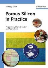
Porous Silicon in Practice (eBook)
XII, 250 Seiten
Wiley-VCH (Verlag)
978-3-527-64192-5 (ISBN)
which can be totally unwilling to settle on smooth silicon surfaces but readily adhere to porous silicon, giving rise to great hopes for such
future applications as programmable drug delivery or advanced, braincontrolled prosthetics. Porous silicon research is active in the fields
of sensors, tissue engineering, medical therapeutics and diagnostics, photovoltaics, rechargeable batteries, energetic materials, photonics,
and MEMS (Micro Electro Mechanical Systems).
Written by an outstanding, well-recognized expert in the field, this book provides detailed, step-by-step instructions to prepare and characterize the major types of porous silicon. It is intended for those new to the fi eld. Sampling of topics covered:
* Principles of Etching Porous Silicon
* Etch Cell Construction and Considerations
* Photonic Crystals, Microcavities, and Bragg Stacks Etched in Silicon
* Preparation of Free-standing Films and Particles of Porous Silicon
* Preparation of Photoluminescent Nanoparticles from Porous Silicon
* Preparation of Silicon Nanowires by Electrochemical Etch of Silicon
* Surface Modifi cation Chemistry and Biochemistry
* Measurement of Optical Properties
* Measurement of Pore Size, Porosity, Thickness, Surface Area
The whole is backed by a generous use of color photographs to illustrate the described procedures in detail, plus a bibliography of further
literature pertinent to a wide range of application fi elds. For materials scientists, chemists, physicists, optical physicists, biomaterials
scientists, neurobiologists, bioengineers, and graduate students in those fields, as well as those working in the semiconductor industry. Einen verständlichen Zugang zum Thema bietet dieser Band und wendet sich an Praktiker ebenso wie an Studierende und Wissenschaftler. Er macht u. a. vertraut mit elektrochemischen Methoden und der Anwendung von Materialien, die zur Herstellung von porösem Silizium notwendig sind.
Michael J. Sailor has been working in the porous silicon field for 20 years. He received a B.S. degree in Chemistry from Harvey Mudd College (Claremont, CA) and a PhD in Chemistry from Northwestern University (Chicago). He holds the position of Professor in the Department of Chemistry and Biochemistry at the University of California, San Diego (UCSD). His research focuses on the chemistry, electrochemistry, and photophysics of porous silicon, emphasizing applications in medical therapeutics and diagnostics, high-throughput screening, and low power sensing of chemical toxins and pollutants.
Preface
FUNDAMENTALS OF POROUS SILICON PREPARATION
Introduction
Chemical Reactions Governing the Dissolution of Silicon
Experimental Set-up and Terminology for Electrochemical Etching of Porous Silicon
Electrochemical Reactions in the Silicon System
Density, Porosity, and Pore Size Definitions
Mechanisms of Electrochemical Dissolution and Pore Formation
Resume of the Properties of Crystalline Silicon
Choosing, Characterizing, and Preparing a Silicon Wafer
PREPARATION OF MICRO-, MESO-, AND MACRO-POROUS SILICON LAYERS
Etch Cell: Materials and Construction
Power Supply
Other Supplies
Safety Precautions and Handling of Waste
Preparing HF Electrolyte Solutions
Cleaning Wafers Prior to Etching
Preparation of Microporous Silicon from a p-Type Wafer
Preparation of Mesoporous Silicon from a p++-Type Wafer
Preparation of Macroporous, Luminescent Porous Silicon from an n-Type Wafer (Frontside Illumination)
Preparation of Macroporous, Luminescent Porous Silicon from an n-Type Wafer (Back Side Illumination)
Preparation of Porous Silicon by Stain Etching
Preparation of Silicon Nanowire Arrays by Metal-Assisted Etching
PREPARATION OF SPATIALLY MODULATED POROUS SILICON LAYERS
Time-Programmable Current Source
Pore Modulation in the z-Direction: Double Layer
Pore Modulation in the z-Direction: Rugate Filter
More Complicated Photonic Devices: Bragg Stacks, Microcavities, and Multi-Line Spectral Filters
Lateral Pore Gradients (in the x-y Plane)
Patterning in the x-y Plane Using Physical or Virtual Masks
Other Patterning Methods
FREESTANDING POROUS SILICON FILMS AND PARTICLES
Freestanding Films of Porous Silicon-"Lift-offs"
Micron-Scale Particles of Porous Silicon by Ultrasonication of Lift-off Films
Core-Shell (Si/SiO2) Nanoparticles of Luminescent Porous Silicon by Ultrasonication
CHARACTERIZATION OF POROUS SILICON
Gravimetric Determination of Porosity and Thickness
Electron Microscopy and Scanned Probe Imaging Methods
Optical Reflectance Measurements
Porosity, Pore Size, and Pore Size Distribution by Nitrogen Adsorption Analysis (BET, BJH, and BdB Methods)
Measurement of Steady-State Photoluminescence Spectra
Time-Resolved Photoluminescence Spectra
Infrared Spectroscopy of Porous Silicon
CHEMISTRY OF POROUS SILICON
Oxide-Forming Reactions of Porous Silicon
Biological Implications of the Aqueous Chemistry of Porous Silicon
Formation of Silicon-Carbon Bonds
Thermal Carbonization Reactions
Conjugation of Biomolecules to Modified Porous Silicon
Chemical Modification in Tandem with Etching
Metallization Reactions of Porous Silicon
APPENDIX A1. ETCH CELL ENGINEERING DIAGRAMS AND SCHEMATICS
Standard or Small Etch Cell-Complete
Standard Etch Cell Top Piece
Small Etch Cell Top Piece
Etch Cell Base (for Either Standard or Small Etch Cell)
Large Etch Cell-Complete
Large Etch Cell Top Piece
Large Etch Cell Base
APPENDIX A2. SAFETY PRECAUTIONS WHEN WORKING WITH HYDROFLUORIC ACID
Hydrofluoric Acid Hazards
First Aid Measures for HF Contact
Note to Physician
HF Antidote Gel
APPENDIX A3. GAS DOSING CELL ENGINEERING DIAGRAMS AND SCHEMATICS
Gas Dosing Cell Top Piece
Gas Dosing Cell Middle Piece
Gas Dosing Cell Bottom Piece Preface
FUNDAMENTALS OF POROUS SILICON PREPARATION
Introduction
Chemical Reactions Governing the Dissolution of Silicon
Experimental Set-up and Terminology for Electrochemical Etching of Porous Silicon
Electrochemical Reactions in the Silicon System
Density, Porosity, and Pore Size Definitions
Mechanisms of Electrochemical Dissolution and Pore Formation
Resume of the Properties of Crystalline Silicon
Choosing, Characterizing, and Preparing a Silicon Wafer
PREPARATION OF MICRO-, MESO-, AND MACRO-POROUS SILICON LAYERS
Etch Cell: Materials and Construction
Power Supply
Other Supplies
Safety Precautions and Handling of Waste
Preparing HF Electrolyte Solutions
Cleaning Wafers Prior to Etching
Preparation of Microporous Silicon from a p-Type Wafer
Preparation of Mesoporous Silicon from a p++-Type Wafer
Preparation of Macroporous, Luminescent Porous Silicon from an n-Type Wafer (Frontside Illumination)
Preparation of Macroporous, Luminescent Porous Silicon from an n-Type Wafer (Back Side Illumination)
Preparation of Porous Silicon by Stain Etching
Preparation of Silicon Nanowire Arrays by Metal-Assisted Etching
PREPARATION OF SPATIALLY MODULATED POROUS SILICON LAYERS
Time-Programmable Current Source
Pore Modulation in the z-Direction: Double Layer
Pore Modulation in the z-Direction: Rugate Filter
More Complicated Photonic Devices: Bragg Stacks, Microcavities, and Multi-Line Spectral Filters
Lateral Pore Gradients (in the x-y Plane)
Patterning in the x-y Plane Using Physical or Virtual Masks
Other Patterning Methods
FREESTANDING POROUS SILICON FILMS AND PARTICLES
Freestanding Films of Porous Silicon-"Lift-offs"
Micron-Scale Particles of Porous Silicon by Ultrasonication of Lift-off Films
Core-Shell (Si/SiO2) Nanoparticles of Luminescent Porous Silicon by Ultrasonication
CHARACTERIZATION OF POROUS SILICON
Gravimetric Determination of Porosity and Thickness
Electron Microscopy and Scanned Probe Imaging Methods
Optical Reflectance Measurements
Porosity, Pore Size, and Pore Size Distribution by Nitrogen Adsorption Analysis (BET, BJH, and BdB Methods)
Measurement of Steady-State Photoluminescence Spectra
Time-Resolved Photoluminescence Spectra
Infrared Spectroscopy of Porous Silicon
CHEMISTRY OF POROUS SILICON
Oxide-Forming Reactions of Porous Silicon
Biological Implications of the Aqueous Chemistry of Porous Silicon
Formation of Silicon-Carbon Bonds
Thermal Carbonization Reactions
Conjugation of Biomolecules to Modified Porous Silicon
Chemical Modification in Tandem with Etching
Metallization Reactions of Porous Silicon
APPENDIX A1. ETCH CELL ENGINEERING DIAGRAMS AND SCHEMATICS
Standard or Small Etch Cell-Complete
Standard Etch Cell Top Piece
Small Etch Cell Top Piece
Etch Cell Base (for Either Standard or Small Etch Cell)
Large Etch Cell-Complete
Large Etch Cell Top Piece
Large Etch Cell Base
APPENDIX A2. SAFETY PRECAUTIONS WHEN WORKING WITH HYDROFLUORIC ACID
Hydrofluoric Acid Hazards
First Aid Measures for HF Contact
Note to Physician
HF Antidote Gel
APPENDIX A3. GAS DOSING CELL ENGINEERING DIAGRAMS AND SCHEMATICS
Gas Dosing Cell Top Piece
Gas Dosing Cell Middle Piece
Gas Dosing Cell Bottom Piece
| Erscheint lt. Verlag | 9.1.2012 |
|---|---|
| Sprache | englisch |
| Themenwelt | Naturwissenschaften ► Chemie ► Anorganische Chemie |
| Technik | |
| Schlagworte | Anorganische Chemie • Chemie • Chemistry • Dünne Schichten, Oberflächen u. Grenzflächen • Dünne Schichten, Oberflächen u. Grenzflächen • Electrical & Electronics Engineering • Electronic materials • Elektronische Materialien • Elektrotechnik u. Elektronik • Festkörperphysik • Festkörperphysik • Halbleiter • Hauptgruppenchemie • Inorganic Chemistry • Main Group Chemistry • Materials Science • Materialwissenschaften • Nanomaterialien • nanomaterials • Nanotechnologie • nanotechnology • Oberflächen- u. Kolloidchemie • Oberflächen- u. Kolloidchemie • Physics • Physik • semiconductors • Silizium • Solid state physics • Surface & Colloid Chemistry • Thin Films, Surfaces & Interfaces |
| ISBN-10 | 3-527-64192-0 / 3527641920 |
| ISBN-13 | 978-3-527-64192-5 / 9783527641925 |
| Haben Sie eine Frage zum Produkt? |
Größe: 20,2 MB
Kopierschutz: Adobe-DRM
Adobe-DRM ist ein Kopierschutz, der das eBook vor Mißbrauch schützen soll. Dabei wird das eBook bereits beim Download auf Ihre persönliche Adobe-ID autorisiert. Lesen können Sie das eBook dann nur auf den Geräten, welche ebenfalls auf Ihre Adobe-ID registriert sind.
Details zum Adobe-DRM
Dateiformat: PDF (Portable Document Format)
Mit einem festen Seitenlayout eignet sich die PDF besonders für Fachbücher mit Spalten, Tabellen und Abbildungen. Eine PDF kann auf fast allen Geräten angezeigt werden, ist aber für kleine Displays (Smartphone, eReader) nur eingeschränkt geeignet.
Systemvoraussetzungen:
PC/Mac: Mit einem PC oder Mac können Sie dieses eBook lesen. Sie benötigen eine
eReader: Dieses eBook kann mit (fast) allen eBook-Readern gelesen werden. Mit dem amazon-Kindle ist es aber nicht kompatibel.
Smartphone/Tablet: Egal ob Apple oder Android, dieses eBook können Sie lesen. Sie benötigen eine
Geräteliste und zusätzliche Hinweise
Buying eBooks from abroad
For tax law reasons we can sell eBooks just within Germany and Switzerland. Regrettably we cannot fulfill eBook-orders from other countries.
aus dem Bereich


