Copper Interconnect Technology (eBook)
XIX, 423 Seiten
Springer New York (Verlag)
978-1-4419-0076-0 (ISBN)
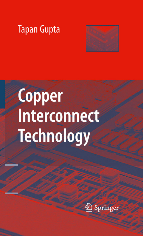
Since overall circuit performance has depended primarily on transistor properties, previous efforts to enhance circuit and system speed were focused on transistors as well. During the last decade, however, the parasitic resistance, capacitance, and inductance associated with interconnections began to influence circuit performance and will be the primary factors in the evolution of nanoscale ULSI technology. Because metallic conductivity and resistance to electromigration of bulk copper (Cu) are better than aluminum, use of copper and low-k materials is now prevalent in the international microelectronics industry. As the feature size of the Cu-lines forming interconnects is scaled, resistivity of the lines increases. At the same time electromigration and stress-induced voids due to increased current density become significant reliability issues. Although copper/low-k technology has become fairly mature, there is no single book available on the promise and challenges of these next-generation technologies. In this book, a leader in the field describes advanced laser systems with lower radiation wavelengths, photolithography materials, and mathematical modeling approaches to address the challenges of Cu-interconnect technology.
Since overall circuit performance has depended primarily on transistor properties, previous efforts to enhance circuit and system speed were focused on transistors as well. During the last decade, however, the parasitic resistance, capacitance, and inductance associated with interconnections began to influence circuit performance and will be the primary factors in the evolution of nanoscale ULSI technology. Because metallic conductivity and resistance to electromigration of bulk copper (Cu) are better than aluminum, use of copper and low-k materials is now prevalent in the international microelectronics industry. As the feature size of the Cu-lines forming interconnects is scaled, resistivity of the lines increases. At the same time electromigration and stress-induced voids due to increased current density become significant reliability issues. Although copper/low-k technology has become fairly mature, there is no single book available on the promise and challenges of these next-generation technologies. In this book, a leader in the field describes advanced laser systems with lower radiation wavelengths, photolithography materials, and mathematical modeling approaches to address the challenges of Cu-interconnect technology.
Preface 6
Acknowledgments 9
Author Biography 15
1 Introduction 16
1.1 Trends and Challenges 17
1.2 Physical Limits and Search for New Materials 20
1.3 Challenges 21
1.4 Choice of Materials 22
1.4.1 Why Copper (Cu) Interconnects? 22
1.4.1.1 Line Resistivity 23
1.4.1.2 Efficiency of Cu-Lines versus Node Technology 25
1.4.1.3 Heat Dissipation 25
1.4.1.4 Electromigration (EM) Failure 26
1.4.1.5 Thermo-Mechanical Properties 27
1.4.1.6 Stress Migration Effect 29
1.5 New Technologies 30
1.5.1 Multilayer Metal Architecture 30
1.5.2 Substrate Engineering 31
1.6 An Alternate Technology for Interconnects 34
1.7 Materials Used in Modern Integrated Circuits 36
1.7.1 Properties of Copper 38
1.7.2 Grain Size 39
1.7.3 Melting Temperature 40
1.8 Barrier Layer 42
1.9 Low-K Dielectric Materials 43
1.10 Polymers 45
1.11 Semiconductors 47
1.11.1 Silicon (Si) 48
1.12 Challenges and Accomplishments 49
1.12.1 Challenges 50
1.12.2 Accomplishments 50
1.13 Technologies of the 21st Century, and the Plan to Meet the Challenges 53
1.14 Ultra-Shallow Junction (USJ) 54
1.15 Circuit Design and Architecture Improvements 56
1.16 Performance and Leakage in Low Standby Power (LSTP) Systems 56
1.17 Introduction of New Materials and Integration Processes 57
1.17.1 Nano-Materials 59
1.17.2 Superconductors 60
1.17.3 Integration Processes 62
1.17.3.1 3-D Technology 62
1.17.3.2 Air Gap Technology 63
1.17.3.3 Fabrication Status of Sub-Micron (65 nm and Below) Devices and Reliability Issues 65
1.18 Summary 68
2 Dielectric Materials 81
2.1 Introduction 81
2.2 Interlayer Dielectric (ILD) 85
2.2.1 Introduction 85
2.2.1.1 Low-K 87
2.2.2 Mathematical Model 88
2.2.3 Selection Criteria for an Ideal Low-K Material 90
2.2.4 Search for an Ideal Low-K Material 92
2.2.4.1 Problems with Porous Films 96
2.2.4.2 Pore Sealing 97
2.2.5 Achievement 97
2.2.5.1 Porous Silicon Dioxide (SiO 2 ) (the Xerogel) 97
2.2.5.2 Carbon Doped Oxide 97
2.2.5.3 Black Diamond 98
2.2.5.4 Bezocyclobutene (BCB) Based Polymer 99
2.2.5.5 Aromatic (Hydrocarbon) Thermosetting Polymer (ATP) 100
2.2.5.6 Hydrogen Silesquioxanes (HSQ, HSiO 1.5 ) 101
2.2.5.7 Methyl Silsesquioxane (MSQ) 103
2.2.5.8 Poly (Arylene Ethers) (PAE) 104
2.2.5.9 Parylene 105
2.2.5.10 Teflon AF 105
2.2.5.11 Diamond-Like Carbon (DLC) 105
2.2.6 Impact of Low-K ILD Materials on the Cu-Damascene Process 106
2.2.7 Deposition Techniques 109
2.2.7.1 Flow chart for Damascene Architecture 109
2.3 High-K Dielectric Materials 110
2.3.1 Introduction 111
2.3.2 Impact on Scaling and Requirements 112
2.3.3 Search for a Suitable High-K Dielectric Material 113
2.3.3.1 Nitrides and Oxynitrides 113
2.3.3.2 Tantalum Oxide (Ta 2 O 5 ) and Titanium Oxide (TiO 2 ) 114
2.3.3.3 Hafnium Oxide (HfO 2 ) 114
2.3.3.4 Zirconium Oxide (ZrO 2 ) 115
2.3.3.5 Lanthanum Aluminate (LaAlO 3 ) 115
2.3.3.6 Titanate Compounds of Barium (BaTiO 3 ), Barium Strontium (BaSrTiO 3 ), and Lead (PbTiO 3 ) 115
2.3.4 Deposition Technology for High-K Materials 116
2.3.5 Summary 116
3 Diffusion and Barrier Layers 125
3.1 Diffusion 125
3.1.1 Introduction 125
3.1.2 Transitional Effects 127
3.1.3 Mathematical Modeling of Diffusion in Cu-Interconnects 128
3.1.4 Grain Boundary (GB) Diffusion 132
3.1.5 Vacancy Diffusion 134
3.1.6 Drift Diffusion 135
3.1.7 Interdiffusion 136
3.1.8 Diffusion of Copper and Its Consequences 136
3.1.9 Precipitation 138
3.2 Barrier Layer for Cu-Interconnects 139
3.2.1 Theory 139
3.2.2 Ideal Barrier Layer 140
3.2.3 Barrier Layer Architecture 140
3.2.4 Interlayer Reactions 142
3.2.4.1 Case I: Single Barrier Layer 143
3.2.4.2 Case II: Double Layer Barrier Cu-Ta-TaN 146
3.2.5 Influence of the Barrier Layer Properties on the Reliability of Cu-Interconnects 146
3.2.5.1 Morphology of the Barrier Layer 146
3.2.5.2 Stress 147
3.2.5.3 Adhesion 148
3.2.6 Low-K Dielectric-Barrier Layer 149
3.2.7 Reaction Rates 149
3.2.7.1 Effect of Ambient 152
3.2.7.2 Processing Temperature 152
3.2.8 Influence of the Barrier Layer on the Electrical Conductivity of Cu-Lines 153
3.2.9 Influence of Barrier Layer Thermal Conductivity on Cu-Line 155
3.2.10 Classification of Barrier Layer 158
3.2.11 Properties of Different Barrier Layer Materials 159
3.2.11.1 Tantalum (Ta) and Its Compounds 159
3.2.11.2 Titanium(Ti) and Its Compounds 160
3.2.11.3 Molybdenum (Mo) and Its Compound 161
3.2.11.4 Tungsten (W) and Its Compounds 161
3.2.11.5 Cobalt 161
3.2.12 Cap-Layer, Its Properties and Functions 162
3.3 Summary 164
4 Pattern Generation 174
4.1 Photolithography 174
4.1.1 Introduction 174
4.1.2 Resolution Limits of Optical Lithography 177
4.1.2.1 Effect of the Media on Resolution 178
4.1.2.2 Effect of Wavelength Exposure on Resolution 179
4.1.2.3 Effect of Numerical Aperture (NA) on Resolution 179
4.1.2.4 Modulation Transfer Function and Critical Dimension (CD) 179
4.1.2.5 Effects of Antireflective Coating (ARC) on Resolution 181
4.1.3 Deep Ultraviolet (DUV) Lithography 181
4.1.3.1 Technology for 193 nm Lithography 182
4.1.3.2 193 nm Exposure System 184
4.1.4 Reticles 186
4.1.5 Enhancement Techniques for Resolution 188
4.1.5.1 Antireflective Coating (ARC) 188
4.1.5.2 Immersion Technique 189
4.1.5.3 Phase Shift Mask (PSM) 190
4.1.6 157 nm Lithography 192
4.1.6.1 Wafer Exposure System 192
4.1.6.2 Optical System for 157 nm Resist 193
4.1.6.3 Reticle and Mask Systems for 157 nm Resist 195
4.1.6.4 Pellicles 196
4.1.7 Chemically Amplified Resist (CA) 196
4.1.8 Extreme Ultraviolet (EUV) Lithography 198
4.1.9 e-Beam Lithography (EBL) 202
4.1.10 Electron-Beam Resist 205
4.1.11 e-Beam Reticle 208
4.1.12 Step and Flash Imprint Lithography (SFIL) 208
4.2 Etching and Cleaning of Damascene Structures 210
4.2.1 Etching 210
4.2.1.1 Advanced Process Technology 210
4.2.1.2 Process Chemistry of Etching 214
4.2.2 Cleaning 223
4.2.2.1 Introduction 223
4.3 Summary 226
5 Deposition Technologies of Materials for Cu-Interconnects 236
5.1 Introduction 236
5.2 Emerging Technologies 237
5.2.1 Cu-Damascene Process 237
5.2.2 Barrier Layer Requirements 238
5.3 Deposition Requirements 238
5.4 Thin Film Growth and Theory of Nucleation 239
5.4.1 Nucleation Theory 240
5.5 Instrumentation 242
5.5.1 Physical Vapor Deposition 243
5.5.2 Sputtering 244
5.5.2.1 DC and RF Sputtering Systems 245
5.5.2.2 Bias Sputtering 245
5.5.2.3 Magnetron Sputtering 246
5.5.2.4 Reactive Sputtering 246
5.5.3 Ionized Physical Vapor Deposition (IPVD) 247
5.6 Chemical Vapor Deposition (CVD) 249
5.6.1 Plasma Enhanced CVD (PECVD) System 249
5.6.2 Metal-Organic Vapor Deposition (MOCVD) 251
5.7 Low Temperature Thermal CVD (LTTCVD) System 253
5.8 Atomic Layer Deposition (ALD) 253
5.9 Plating 256
5.9.1 History of Electroplating and Printed Circuit Boards (PCBs) 256
5.9.2 DC Bath Chemistry 257
5.9.3 Electroplating of Copper Inside Damascene Architecture 258
5.10 Process Chemistry for Superconformal Electrodeposition of Copper 260
5.11 Electrochemical Mechanical Deposition (ECMD) 260
5.12 Influence of the Seed Layer on Electroplating 261
5.13 Electroless Deposition of Copper 263
5.14 Stress in Cu-Interconnects 263
5.15 Summary 265
6 The Copper Damascene Process and Chemical Mechanical Polishing 279
6.1 The Copper Damascene Process 279
6.1.1 Introduction 279
6.1.2 Conventional Metallization Technology 282
6.1.3 Cu-Damascene Metallization Technology 283
6.1.3.1 Different Approaches to Cu-Damascene Metallization 285
6.1.4 General Objectives and Challenges 288
6.2 Chemical Mechanical Polishing (CMP) and Planarization 290
6.2.1 Introduction 290
6.2.2 Chemical Mechanical Polishing (CMP)Technology 291
6.2.2.1 An Analytical Model 294
6.2.3 Copper Dishing Model 297
6.2.4 Slurry Chemistry 298
6.2.5 Particle Size Inside the Slurry 299
6.2.6 Relative Velocity of the Pad and Wafer 301
6.2.7 Pad Pressure 301
6.2.8 Pad-Elasticity 301
6.2.9 Pad Conditioning 301
6.2.10 Shallow Trench Isolation (STI) 302
6.2.11 Abrasive Free Polishing 303
6.2.12 End-Point Detection 303
6.2.13 Dry In Dry Out 304
6.2.14 Multi-Step Processing 305
6.2.15 Post-CMP Cleaning 305
6.2.16 CMP Pattern Density Issues 307
6.3 Summary 307
7 Conduction and Electromigration 313
7.1 Conduction 313
7.1.1 Introduction 313
7.1.2 Conduction Mechanism and Restrictions 315
7.1.2.1 Scattering and Its Influence on Coductivity 316
7.1.2.2 Grain Boundary (GB) Scattering 320
7.1.2.3 Effective Resistance of Cu-Interconnect Due to Different Size of the Grains and the Presence of Barrier Layer 322
7.1.3 Effect of Grain Boundary (GB) Resistance on the Conductivity of Cu-Interconnects 323
7.1.4 Effect of Grain Size and Morphology of the Substrate 323
7.1.5 Morphology of the Cu-Film and Its Influence on the Conduction (Electrical) Mechanism of Cu-Interconnects 324
7.1.6 Effect of Film Thickness on the Conductivity of Cu-Interconnects 329
7.1.7 Diffusion Related Impacts on the Conductivity of a Cu-Line 330
7.1.8 Cu-Line Stress and Its Consequences 331
7.1.8.1 Stress Evolution Related Resistivity 332
7.1.9 Conduction of Heat Through Cu-Interconnects 333
7.1.10 Thermal Cycling (Annealing) Related Phenomena 334
7.2 Electromigration (EM) 336
7.2.1 Electromigration (EM) 336
7.2.2 Mechanism of Electromigration (EM) and Its Effects 337
7.2.3 Void Formation 341
7.2.4 Analytical Model on Stress Related EM 342
7.2.5 Effect of Microstructure of the Film on Mass Migration 345
7.2.6 Effect of Solute on Electromigration 347
7.2.7 Melting Temperature of a Metal and Its Effect on Grain Growth 347
7.2.8 Effect of Temperature on EM 348
7.2.9 Current Density and Its Effect on EM 348
7.3 Summary 348
8 Routing and Reliability 358
8.1 Routing 358
8.1.1 Introduction 358
8.1.2 Methods of Improving Interconnect Routings 360
8.1.2.1 Materials 360
8.1.2.2 Process Integration 362
8.1.2.3 Advanced Lithography 362
8.1.3 Interconnect Routing Design 362
8.1.3.1 Repeater Design 362
8.1.3.2 Bit Line 365
8.1.3.3 Scaling and Design 365
8.1.3.4 Manhattan Design 367
8.1.3.5 X-Architecture 367
8.1.3.6 Multilevel Design 369
8.1.4 Challenges with High Density Routing 370
8.1.4.1 Noise 370
8.1.4.2 Cross-Talk 370
8.1.5 Cascaded Driver 372
8.1.6 Transmission Line Coupling 372
8.1.7 Clocking of High-Speed System 372
8.2 Reliability 373
8.2.1 Introduction 373
8.2.2 Reliability Issues Related to Cu-Interconnects 376
8.2.2.1 Deposition Process Related Issues 376
8.2.2.2 Seed-Layer Related Reliability Issues 377
8.2.2.3 Oxidation Related Problems 378
8.2.2.4 Adhesion Problem 379
8.2.2.5 Scattering Related Reliability Issues 380
8.2.2.6 Joule Heating and Reliability Issues 381
8.2.2.7 Stress in Cu-Line and Its Effects on Reliability Issues 382
8.2.2.8 Thermal Stress and Related Phenomena 383
8.2.2.9 Blech Effect and Its Consequences 384
8.2.2.10 Reliability Problems Due to Electromigration (EM) 385
8.2.2.11 Void Formation and Reliability Issues 387
8.2.2.12 Diffusion Related Problems 388
8.2.2.13 Reliability of the Barrier Layer 388
8.2.2.14 Presence of Via Holes and Trenches and Reliability Related Problems 390
8.2.2.15 Reliability of the Low-K Materials 391
8.2.2.16 Impact of Exotic Materials on Dual-Damascene Pattern Formation 394
8.2.2.17 Etching Processes and the Reliability 395
8.2.2.18 Reliability of Chemical-Mechanical Polishing (CMP) 396
8.2.2.19 Cleaning Process and Reliability 397
8.2.3 Measurements 399
8.3 Summary 402
Glossary (Copper Interconnects) 415
Index 425
| Erscheint lt. Verlag | 22.1.2010 |
|---|---|
| Zusatzinfo | XIX, 423 p. |
| Verlagsort | New York |
| Sprache | englisch |
| Themenwelt | Technik ► Elektrotechnik / Energietechnik |
| Technik ► Maschinenbau | |
| Schlagworte | circuit performance • copper/low-k technology • cu interconnect technology • Electronics • electronics packaging • electronics packaging reliability • Laser • Material • nanoscale usli technology • nanostructured copper interconnects • parasitic resistance, capacit • parasitic resistance, capacitance, and inductance |
| ISBN-10 | 1-4419-0076-4 / 1441900764 |
| ISBN-13 | 978-1-4419-0076-0 / 9781441900760 |
| Haben Sie eine Frage zum Produkt? |
Größe: 12,1 MB
DRM: Digitales Wasserzeichen
Dieses eBook enthält ein digitales Wasserzeichen und ist damit für Sie personalisiert. Bei einer missbräuchlichen Weitergabe des eBooks an Dritte ist eine Rückverfolgung an die Quelle möglich.
Dateiformat: PDF (Portable Document Format)
Mit einem festen Seitenlayout eignet sich die PDF besonders für Fachbücher mit Spalten, Tabellen und Abbildungen. Eine PDF kann auf fast allen Geräten angezeigt werden, ist aber für kleine Displays (Smartphone, eReader) nur eingeschränkt geeignet.
Systemvoraussetzungen:
PC/Mac: Mit einem PC oder Mac können Sie dieses eBook lesen. Sie benötigen dafür einen PDF-Viewer - z.B. den Adobe Reader oder Adobe Digital Editions.
eReader: Dieses eBook kann mit (fast) allen eBook-Readern gelesen werden. Mit dem amazon-Kindle ist es aber nicht kompatibel.
Smartphone/Tablet: Egal ob Apple oder Android, dieses eBook können Sie lesen. Sie benötigen dafür einen PDF-Viewer - z.B. die kostenlose Adobe Digital Editions-App.
Zusätzliches Feature: Online Lesen
Dieses eBook können Sie zusätzlich zum Download auch online im Webbrowser lesen.
Buying eBooks from abroad
For tax law reasons we can sell eBooks just within Germany and Switzerland. Regrettably we cannot fulfill eBook-orders from other countries.
aus dem Bereich


