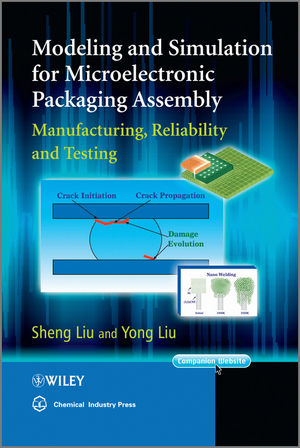
Modeling and Simulation for Microelectronic Packaging Assembly
John Wiley & Sons Inc (Verlag)
978-0-470-82780-2 (ISBN)
- Lieferbar (Termin unbekannt)
- Versandkostenfrei innerhalb Deutschlands
- Auch auf Rechnung
- Verfügbarkeit in der Filiale vor Ort prüfen
- Artikel merken
Although there is increasing need for modeling and simulation in the IC package design phase, most assembly processes and various reliability tests are still based on the time consuming "test and try out" method to obtain the best solution. Modeling and simulation can easily ensure virtual Design of Experiments (DoE) to achieve the optimal solution. This has greatly reduced the cost and production time, especially for new product development. Using modeling and simulation will become increasingly necessary for future advances in 3D package development. In this book, Liu and Liu allow people in the area to learn the basic and advanced modeling and simulation skills to help solve problems they encounter.
Models and simulates numerous processes in manufacturing, reliability and testing for the first time
Provides the skills necessary for virtual prototyping and virtual reliability qualification and testing
Demonstrates concurrent engineering and co-design approaches for advanced engineering design of microelectronic products
Covers packaging and assembly for typical ICs, optoelectronics, MEMS, 2D/3D SiP, and nano interconnects
Appendix and color images available for download from the book's companion website
Liu and Liu have optimized the book for practicing engineers, researchers, and post-graduates in microelectronic packaging and interconnection design, assembly manufacturing, electronic reliability/quality, and semiconductor materials. Product managers, application engineers, sales and marketing staff, who need to explain to customers how the assembly manufacturing, reliability and testing will impact their products, will also find this book a critical resource.
Appendix and color version of selected figures can be found at www.wiley.com/go/liu/packaging
Sheng Liu is a ChangJiang Professor of Mechanical Engineering at Huazhong University of Science and Technology. He holds a dual appointment at Wuhan National Laboratory for Optoelectronics, and has served as tenured faculty at Wayne State University. He has over 14 years experience in LED/MEMS/IC packaging and extensive experience in consulting with many leading multi-national and Chinese companies. Liu was awarded the White House/NSF Presidential Faculty Fellowship in 1995, ASME Young Engineer Award in 1996, and China NSFC Overseas Young Scientist in 1999. He is currently one of the 11 National Committee Members in LED under Ministry of Science and Technology. He obtained a Ph.D. from Stanford in 1992, and got MS and BS in flight vehicle design, Nanjing University of Aeronautics and Astronautics, and he had three years industrial experience in China and USA. He has filed more than 70 patents in China and the USA, and has published more than 300 technical articles. Yong Liu is a global team leader of electrical, thermal-mechanical modeling and analysis at Fairchild Semiconductor Corp in South Portland, Maine. His main interest areas are IC packaging, modeling and simulation, reliability and material characterization. He has previously served as Professor at Zhejiang University of Technology, and has worked as an opto package engineer at Nortel Networks in Boston. Liu has co-authored over 100 papers in journals and conferences, has filed over 40 US patents in the area of IC packaging and power device, and has won numerous awards and fellowships in academia and industry: the Fairchild President Award, Fairchild Key Technologist, Fairchild New Product Innovation Award, the Alexander von Humboldt European Fellowship for study at Braunschweig University of Technology and University of Cambridge. Liu holds a PhD from Nanjing University of Science and Technology.
Foreword by C. P. Wong xiii Foreword by Zhigang Suo xv
Preface xvii
Acknowledgments xix
About the Authors xxi
Part I Mechanics and Modeling 1
1 Constitutive Models and Finite Element Method 3
1.1 Constitutive Models for Typical Materials 3
1.1.1 Linear Elasticity 3
1.1.2 Elastic-Visco-Plasticity 5
1.2 Finite Element Method 9
1.2.1 Basic Finite Element Equations 9
1.2.2 Nonlinear Solution Methods 12
1.2.3 Advanced Modeling Techniques in Finite Element Analysis 14
1.2.4 Finite Element Applications in Semiconductor Packaging Modeling 17
1.3 Chapter Summary 18
References 19
2 Material and Structural Testing for Small Samples 21
2.1 Material Testing for Solder Joints 21
2.1.1 Specimens 21
2.1.2 A Thermo-Mechanical Fatigue Tester 23
2.1.3 Tensile Test 24
2.1.4 Creep Test 26
2.1.5 Fatigue Test 31
2.2 Scale Effect of Packaging Materials 32
2.2.1 Specimens 33
2.2.2 Experimental Results and Discussions 34
2.2.3 Thin Film Scale Dependence for Polymer Thin Films 39
2.3 Two-Ball Joint Specimen Fatigue Testing 41
2.4 Chapter Summary 41
References 43
3 Constitutive and User-Supplied Subroutines for Solders Considering Damage Evolution 45
3.1 Constitutive Model for Tin-Lead Solder Joint 45
3.1.1 Model Formulation 45
3.1.2 Determination of Material Constants 47
3.1.3 Model Prediction 49
3.2 Visco-Elastic-Plastic Properties and Constitutive Modeling of Underfills 50
3.2.1 Constitutive Modeling of Underfills 50
3.2.2 Identification of Material Constants 55
3.2.3 Model Verification and Prediction 55
3.3 A Damage Coupling Framework of Unified Viscoplasticity for the Fatigue of Solder Alloys 56
3.3.1 Damage Coupling Thermodynamic Framework 56
3.3.2 Large Deformation Formulation 62
3.3.3 Identification of the Material Parameters 63
3.3.4 Creep Damage 66
3.4 User-Supplied Subroutines for Solders Considering Damage Evolution 67
3.4.1 Return-Mapping Algorithm and FEA Implementation 67
3.4.2 Advanced Features of the Implementation 69
3.4.3 Applications of the Methodology 71
3.5 Chapter Summary 76
References 76
4 Accelerated Fatigue Life Assessment Approaches for Solders in Packages 79
4.1 Life Prediction Methodology 79
4.1.1 Strain-Based Approach 80
4.1.2 Energy-Based Approach 82
4.1.3 Fracture Mechanics-Based Approach 82
4.2 Accelerated Testing Methodology 82
4.2.1 Failure Modes via Accelerated Testing Bounds 83
4.2.2 Isothermal Fatigue via Thermal Fatigue 83
4.3 Constitutive Modeling Methodology 83
4.3.1 Separated Modeling via Unified Modeling 83
4.3.2 Viscoplasticity with Damage Evolution 84
4.4 Solder Joint Reliability via FEA 84
4.4.1 Life Prediction of Ford Joint Specimen 84
4.4.2 Accelerated Testing: Insights from Life Prediction 87
4.4.3 Fatigue Life Prediction of a PQFP Package 91
4.5 Life Prediction of Flip-Chip Packages 93
4.5.1 Fatigue Life Prediction with and without Underfill 93
4.5.2 Life Prediction of Flip-Chips without Underfill via Unified and Separated Constitutive Modeling 95
4.5.3 Life Prediction of Flip-Chips under Accelerated Testing 96
4.6 Chapter Summary 99
References 99
5 Multi-Physics and Multi-Scale Modeling 103
5.1 Multi-Physics Modeling 103
5.1.1 Direct-Coupled Analysis 103
5.1.2 Sequential Coupling 104
5.2 Multi-Scale Modeling 106
5.3 Chapter Summary 107
References 108
6 Modeling Validation Tools 109
6.1 Structural Mechanics Analysis 109
6.2 Requirements of Experimental Methods for Structural Mechanics Analysis 111
6.3 Whole Field Optical Techniques 112
6.4 Thermal Strains Measurements Using Moire Interferometry 113
6.4.1 Thermal Strains in a Plastic Ball Grid Array (PBGA) Interconnection 113
6.4.2 Real-Time Thermal Deformation Measurements Using Moire Interferometry 116
6.5 In-Situ Measurements on Micro-Machined Sensors 116
6.5.1 Micro-Machined Membrane Structure in a Chemical Sensor 116
6.5.2 In-Situ Measurement Using Twyman–Green Interferometry 118
6.5.3 Membrane Deformations due to Power Cycles 118
6.6 Real-Time Measurements Using Speckle Interferometry 119
6.7 Image Processing and Computer Aided Optical Techniques 120
6.7.1 Image Processing for Fringe Analysis 120
6.7.2 Phase Shifting Technique for Increasing Displacement Resolution 120
6.8 Real-Time Thermal-Mechanical Loading Tools 123
6.8.1 Micro-Mechanical Testing 123
6.8.2 Environmental Chamber 124
6.9 Warpage Measurement Using PM-SM System 124
6.9.1 Shadow Moire and Project Moire Setup 125
6.9.2 Warpage Measurement of a BGA, Two Crowded PCBs 127
6.10 Chapter Summary 131
References 131
7 Application of Fracture Mechanics 135
7.1 Fundamental of Fracture Mechanics 135
7.1.1 Energy Release Rate 136
7.1.2 J Integral 138
7.1.3 Interfacial Crack 139
7.2 Bulk Material Cracks in Electronic Packages 141
7.2.1 Background 141
7.2.2 Crack Propagation in Ceramic/Adhesive/Glass System 142
7.2.3 Results 146
7.3 Interfacial Fracture Toughness 148
7.3.1 Background 148
7.3.2 Interfacial Fracture Toughness of Flip-Chip Package between Passivated Silicon Chip and Underfill 150
7.4 Three-Dimensional Energy Release Rate Calculation 159
7.4.1 Fracture Analysis 160
7.4.2 Results and Comparison 160
7.5 Chapter Summary 165
References 165
8 Concurrent Engineering for Microelectronics 169
8.1 Design Optimization 169
8.2 New Developments and Trends in Integrated Design Tools 179
8.3 Chapter Summary 183
References 183
Part II Modeling in Microelectronic Packaging and Assembly 185
9 Typical IC Packaging and Assembly Processes 187
9.1 Wafer Process and Thinning 188
9.1.1 Wafer Process Stress Models 188
9.1.2 Thin Film Deposition 189
9.1.3 Backside Grind for Thinning 191
9.2 Die Pick Up 193
9.3 Die Attach 198
9.3.1 Material Constitutive Relations 200
9.3.2 Modeling and Numerical Strategies 201
9.3.3 FEA Simulation Result of Flip-Chip Attach 204
9.4 Wire Bonding 206
9.4.1 Assumption, Material Properties and Method of Analysis 207
9.4.2 Wire Bonding Process with Different Parameters 208
9.4.3 Impact of Ultrasonic Amplitude 210
9.4.4 Impact of Ultrasonic Frequency 212
9.4.5 Impact of Friction Coefficients between Bond Pad and FAB 214
9.4.6 Impact of Different Bond Pad Thickness 217
9.4.7 Impact of Different Bond Pad Structures 217
9.4.8 Modeling Results and Discussion for Cooling Substrate Temperature after Wire Bonding 221
9.5 Molding 223
9.5.1 Molding Flow Simulation 223
9.5.2 Curing Stress Model 230
9.5.3 Molding Ejection and Clamping Simulation 236
9.6 Leadframe Forming/Singulation 241
9.6.1 Euler Forward versus Backward Solution Method 242
9.6.2 Punch Process Setup 242
9.6.3 Punch Simulation by ANSYS Implicit 244
9.6.4 Punch Simulation by LS-DYNA 246
9.6.5 Experimental Data 248
9.7 Chapter Summary 252
References 252
10 Opto Packaging and Assembly 255
10.1 Silicon Substrate Based Opto Package Assembly 255
10.1.1 State of the Technology 255
10.1.2 Monte Carlo Simulation of Bonding/Soldering Process 256
10.1.3 Effect of Matching Fluid 256
10.1.4 Effect of the Encapsulation 258
10.2 Welding of a Pump Laser Module 258
10.2.1 Module Description 258
10.2.2 Module Packaging Process Flow 258
10.2.3 Radiation Heat Transfer Modeling for Hermetic Sealing Process 259
10.2.4 Two-Dimensional FEA Modeling for Hermetic Sealing 260
10.2.5 Cavity Radiation Analyses Results and Discussions 262
10.3 Chapter Summary 264
References 264
11 MEMS and MEMS Package Assembly 267
11.1 A Pressure Sensor Packaging (Deformation and Stress) 267
11.1.1 Piezoresistance in Silicon 268
11.1.2 Finite Element Modeling and Geometry 270
11.1.3 Material Properties 270
11.1.4 Results and Discussion 271
11.2 Mounting of Pressure Sensor 273
11.2.1 Mounting Process 273
11.2.2 Modeling 274
11.2.3 Results 276
11.2.4 Experiments and Discussions 277
11.3 Thermo-Fluid Based Accelerometer Packaging 279
11.3.1 Device Structure and Operation Principle 279
11.3.2 Linearity Analysis 280
11.3.3 Design Consideration 284
11.3.4 Fabrication 285
11.3.5 Experiment 285
11.4 Plastic Packaging for a Capacitance Based Accelerometer 288
11.4.1 Micro-Machined Accelerometer 289
11.4.2 Wafer-Level Packaging 290
11.4.3 Packaging of Capped Accelerometer 296
11.5 Tire Pressure Monitoring System (TPMS) Antenna 303
11.5.1 Test of TPMS System with Wheel Antenna 304
11.5.2 3D Electromagnetic Modeling of Wheel Antenna 306
11.5.3 Stress Modeling of Installed TPMS 307
11.6 Thermo-Fluid Based Gyroscope Packaging 310
11.6.1 Operating Principle and Design 312
11.6.2 Analysis of Angular Acceleration Coupling 313
11.6.3 Numerical Simulation and Analysis 314
11.7 Microjets for Radar and LED Cooling 316
11.7.1 Microjet Array Cooling System 319
11.7.2 Preliminary Experiments 320
11.7.3 Simulation and Model Verification 322
11.7.4 Comparison and Optimization of Three Microjet Devices 324
11.8 Air Flow Sensor 327
11.8.1 Operation Principle 329
11.8.2 Simulation of Flow Conditions 331
11.8.3 Simulation of Temperature Field on the Sensor Chip Surface 333
11.9 Direct Numerical Simulation of Particle Separation by Direct Current Dielectrophoresis 335
11.9.1 Mathematical Model and Implementation 335
11.9.2 Results and Discussion 339
11.10 Modeling of Micro-Machine for Use in Gastrointestinal Endoscopy 341
11.10.1 Methods 343
11.10.2 Results and Discussion 348
11.11 Chapter Summary 353
References 354
12 System in Package (SIP) Assembly 361
12.1 Assembly Process of Side by Side Placed SIP 361
12.1.1 Multiple Die Attach Process 361
12.1.2 Cooling Stress and Warpage Simulation after Molding 365
12.1.3 Stress Simulation in Trim Process 366
12.2 Impact of the Nonlinear Materials Behaviors on the Flip-Chip Packaging Assembly Reliability 369
12.2.1 Finite Element Modeling and Effect of Material Models 371
12.2.2 Experiment 374
12.2.3 Results and Discussions 375
12.3 Stacked Die Flip-Chip Assembly Layout and the Material Selection 381
12.3.1 Finite Element Model for the Stack Die FSBGA 383
12.3.2 Assembly Layout Investigation 385
12.3.3 Material Selection 389
12.4 Chapter Summary 393
References 393
Part III Modeling in Microelectronic Package Reliability and Test 395
13 Wafer Probing Test 397
13.1 Probe Test Model 397
13.2 Parameter Probe Test Modeling Results and Discussions 400
13.2.1 Impact of Probe Tip Geometry Shapes 401
13.2.2 Impact of Contact Friction 403
13.2.3 Impact of Probe Tip Scrub 403
13.3 Comparison Modeling: Probe Test versus Wire Bonding 406
13.4 Design of Experiment (DOE) Study and Correlation of Probing Experiment and FEA Modeling 409
13.5 Chapter Summary 411
References 412
14 Power and Thermal Cycling, Solder Joint Fatigue Life 413
14.1 Die Attach Process and Material Relations 413
14.2 Power Cycling Modeling and Discussion 413
14.3 Thermal Cycling Modeling and Discussion 420
14.4 Methodology of Solder Joint Fatigue Life Prediction 426
14.5 Fatigue Life Prediction of a Stack Die Flip-Chip on Silicon (FSBGA) 427
14.6 Effect of Cleaned and Non-Cleaned Situations on the Reliability of Flip-Chip Packages 434
14.6.1 Finite Element Models for the Clean and Non-Clean Cases 435
14.6.2 Model Evaluation 435
14.6.3 Reliability Study for the Solder Joints 437
14.7 Chapter Summary 438
References 439
15 Passivation Crack Avoidance 441
15.1 Ratcheting-Induced Stable Cracking: A Synopsis 441
15.2 Ratcheting in Metal Films 445
15.3 Cracking in Passivation Films 447
15.4 Design Modifications 452
15.5 Chapter Summary 452
References 452
16 Drop Test 453
16.1 Controlled Pulse Drop Test 453
16.1.1 Simulation Methods 454
16.1.2 Simulation Results 457
16.1.3 Parametric Study 458
16.2 Free Drop 460
16.2.1 Simulated Drop Test Procedure 460
16.2.2 Modeling Results and Discussion 461
16.3 Portable Electronic Devices Drop Test and Simulation 467
16.3.1 Test Set-Up 467
16.3.2 Modeling and Simulation 468
16.3.3 Results 470
16.4 Chapter Summary 470
References 471
17 Electromigration 473
17.1 Basic Migration Formulation and Algorithm 473
17.2 Electromigration Examples from IC Device and Package 477
17.2.1 A Sweat Structure 477
17.2.2 A Flip-Chip CSP with Solder Bumps 480
17.3 Chapter Summary 496
References 497
18 Popcorning in Plastic Packages 499
18.1 Statement of Problem 499
18.2 Analysis 501
18.3 Results and Comparisons 503
18.3.1 Behavior of a Delaminated Package due to Pulsed Heating-Verification 503
18.3.2 Convergence of the Total Strain Energy Release Rate 504
18.3.3 Effect of Delamination Size and Various Processes for a Thick Package 505
18.3.4 Effect of Moisture Expansion Coefficient 514
18.4 Chapter Summary 515
References 516
Part IV Modern Modeling and Simulation Methodologies: Application to Nano Packaging 519
19 Classical Molecular Dynamics 521
19.1 General Description of Molecular Dynamics Method 521
19.2 Mechanism of Carbon Nanotube Welding onto the Metal 522
19.2.1 Computational Methodology 522
19.2.2 Results and Discussion 523
19.3 Applications of Car–Parrinello Molecular Dynamics 530
19.3.1 Car–Parrinello Simulation of Initial Growth Stage of Gallium Nitride on Carbon Nanotube 530
19.3.2 Effects of Mechanical Deformation on Outer Surface Reactivity of Carbon Nanotubes 534
19.3.3 Adsorption Configuration of Magnesium on Wurtzite Gallium Nitride Surface Using First-Principles Calculations 539
19.4 Nano-Welding by RF Heating 544
19.5 Chapter Summary 548
References 548
Index 553
| Verlagsort | New York |
|---|---|
| Sprache | englisch |
| Maße | 175 x 252 mm |
| Gewicht | 1134 g |
| Themenwelt | Technik ► Elektrotechnik / Energietechnik |
| Technik ► Maschinenbau | |
| ISBN-10 | 0-470-82780-7 / 0470827807 |
| ISBN-13 | 978-0-470-82780-2 / 9780470827802 |
| Zustand | Neuware |
| Haben Sie eine Frage zum Produkt? |
aus dem Bereich


