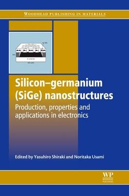
Silicon-Germanium (SiGe) Nanostructures
Woodhead Publishing Ltd (Verlag)
978-1-84569-689-4 (ISBN)
- Keine Verlagsinformationen verfügbar
- Artikel merken
Nanostructured silicon-germanium (SiGe) opens up the prospects of novel and enhanced electronic device performance, especially for semiconductor devices. Silicon-germanium (SiGe) nanostructures reviews the materials science of nanostructures and their properties and applications in different electronic devices.
The introductory part one covers the structural properties of SiGe nanostructures, with a further chapter discussing electronic band structures of SiGe alloys. Part two concentrates on the formation of SiGe nanostructures, with chapters on different methods of crystal growth such as molecular beam epitaxy and chemical vapour deposition. This part also includes chapters covering strain engineering and modelling. Part three covers the material properties of SiGe nanostructures, including chapters on such topics as strain-induced defects, transport properties and microcavities and quantum cascade laser structures. In Part four, devices utilising SiGe alloys are discussed. Chapters cover ultra large scale integrated applications, MOSFETs and the use of SiGe in different types of transistors and optical devices.
With its distinguished editors and team of international contributors, Silicon-germanium (SiGe) nanostructures is a standard reference for researchers focusing on semiconductor devices and materials in industry and academia, particularly those interested in nanostructures.
Yasuhiro Shiraki is X at Tokyo City University, Japan. Noritaka Usami is an Associate Professor at the Institute for Materials Research, Tohoku University, Japan.
Contributor contact details
Preface
Part I: Introduction
Chapter 1: Structural properties of silicon–germanium (SiGe) nanostructures
Abstract:
1.1 Introduction
1.2 Crystal structure
1.3 Lattice parameters
1.4 Phase diagram
1.5 Critical thickness
1.6 Structural characterization by X-ray diffraction
1.7 Future trends
1.8 Acknowledgement
Chapter 2: Electronic band structures of silicon–germanium (SiGe) alloys
Abstract:
2.1 Band structures
2.2 Strain effects
2.3 Effective mass
2.4 Conclusion
Part II: Formation of nanostructures
Chapter 3: Understanding crystal growth mechanisms in silicon–germanium (SiGe) nanostructures
Abstract:
3.1 Introduction
3.2 Thermodynamics of crystal growth
3.3 Fundamental growth processes
3.4 Kinetics of epitaxial growth
3.5 Heteroepitaxy
Chapter 4: Types of silicon–germanium (SiGe) bulk crystal growth methods and their applications
Abstract:
4.1 Introduction
4.2 Growth methods
4.3 Application of silicon–germanium (SiGe) bulk crystal to heteroepitaxy
4.4 Conclusion
Chapter 5: Silicon–germanium (SiGe) crystal growth using molecular beam epitaxy
Abstract:
5.1 Introduction
5.2 Techniques
5.3 Nanostructure formation by molecular bean epitaxy (MBE)
5.4 Future trends
Chapter 6: Silicon–germanium (SiGe) crystal growth using chemical vapor deposition
Abstract:
6.1 Introduction
6.2 Epitaxial growth techniques – chemical vapor deposition (CVD) (ultra high vacuum CVD (UHVCVD), low pressure CVD (LPCVD), atmospheric pressure CVD (APCVD), plasma enhanced CVD (PECVD))
6.3 Silicon–germanium (SiGe) heteroepitaxy by chemical vapor deposition (CVD)
6.4 Doping of silicon–germanium (SiGe)
6.5 Conclusion and future trends
Chapter 7: Strain engineering of silicon–germanium (SiGe) virtual substrates
Abstract:
7.1 Introduction
7.2 Compositionally graded buffer
7.3 Low-temperature buffer
7.4 Ion-implantation buffer
7.5 Other methods and future trends
Chapter 8: Formation of silicon–germanium on insulator (SGOI) substrates
Abstract:
8.1 Introduction: demand for virtual substrate and (Si)Ge on insulator (SGOI)
8.2 Formation of (Si)Ge on insulator (SGOI) by the Ge condensation method
8.3 Extension toward Ge on insulator
8.4 Conclusion
8.5 Acknowledgment
Chapter 9: Miscellaneous methods and materials for silicon–germanium (SiGe) based heterostructures
Abstract:
9.1 Introduction
9.2 Oriented growth of silicon-germanium (SiGe)on insulating films for thin film transistors and 3-D stacked devices
9.3 Heteroepitaxial growth of ferromagnetic Heusler alloys for silicon-germanium (SiGe)-based spintronic devices
9.4 Conclusion
Chapter 10: Modeling the evolution of germanium islands on silicon(001) thin films
Abstract:
10.1 A few considerations on epitaxial growth modeling
10.2 Introduction to Stranski–Krastanow (SK) heteroepitaxy
10.3 Onset of Stranski–Krastanow (SK) heteroepitaxy
10.4 Beyond the Stranski–Krastranow (SK) onset: SiGe intermixing
10.5 Beyond the Stranski–Krastanow (SK) onset: vertical and horizontal ordering for applications
10.6 Future trends: ordering Ge islands on pit-patterned Si(001)
Chapter 11: Strain engineering of silicon–germanium (SiGe) micro- and nanostructures
Abstract:
11.1 Introduction
11.2 Growth insights
11.3 Island engineering
11.4 Rolled-up nanotechnology
11.5 Potential applications
11.6 Sources of further information and advice
11.7 Acknowledgments
Part III: Material properties of SiGe nanostructures
Chapter 12: Self-diffusion and dopant diffusion in germanium (Ge) and silicon–germanium (SiGe) alloys
Abstract:
12.1 Introduction
12.2 Diffusion mechanism
12.3 Self-diffusion in germanium (Ge)
12.4 Self-diffusion in silicon–germanium (SiGe) alloys
12.5 Silicon-germanium (Si–Ge) interdiffusion
12.6 Dopant diffusion in germanium (Ge)
12.7 Dopant diffusion in silicon–germanium (SiGe) alloys
12.8 Dopant segregation
12.9 Conclusion and future trends
Chapter 13: Dislocations and other strain-induced defects in silicon–germanium (SiGe) nanostructures
Abstract:
13.1 Introduction and background
13.2 Historical overview
13.3 Application of the Thompson tetrahedron to extended defects in silicon–germanium (SiGe)
13.4 Current topics
13.5 Future trends
13.6 Acknowledgments
Chapter 14: Transport properties of silicon/silicon–germanium (Si/SiGe) nanostructures at low temperatures
Abstract:
14.1 Introduction
14.2 Model, disorder and transport theory
14.3 Transport in quantum wells
14.4 Transport in heterostructures
14.5 Comparison with experimental results
14.6 Discussion and future trends
14.7 Conclusions
14.8 Acknowledgements
Chapter 15: Transport properties of silicon–germanium (SiGe) nanostructures and applications in devices
Abstract:
15.1 Introduction
15.2 Basic transport properties of strained silicon–germanium (SiGe) heterostructures
15.3 Strain engineering
15.4 Low-dimensional transport
15.5 Carrier transport in silicon/silicon–germanium (Si/SiGe) devices
15.6 Future trends
Chapter 16: Microcavities and quantum cascade laser structures based on silicon–germanium (SiGe) nanostructures
Abstract:
16.1 Introduction
16.2 Germanium (Ge) dots microcavity photonic devices
16.3 Silicon–germanium (SiGe) quantum cascade laser (QCL) structures
16.4 Conclusions
Chapter 17: Silicide and germanide technology for interconnections in ultra-large-scale integrated (ULSI) applications
Abstract:
17.1 Introduction
17.2 Formation of silicide and germanosilicide thin films
17.3 Crystalline properties of silicides
17.4 Electrical properties
Part IV: Devices using silicon, germanium and silicon–germanium (Si, Ge and SiGe) alloys
Chapter 18: Silicon–germanium (SiGe) heterojunction bipolar transistor (HBT) and bipolar complementary metal oxide semiconductor (BiCMOS) technologies
Abstract:
18.1 Introduction
18.2 Epitaxial growth
18.3 Silicon–germanium (SiGe) heterojunction bipolar transistor (HBT)
18.4 Silicon–germanium (SiGe) bipolar complementary metal oxide semiconductors (BiCMOS)
18.5 Applications in integrated circuit (IC) and large-scale integration (LSI)
18.6 Conclusion
Chapter 19: Silicon–germanium (SiGe)-based field effect transistors (FET) and complementary metal oxide semiconductor (CMOS) technologies
Abstract:
19.1 Introduction
19.2 Silicon–germanium (SiGe) channel metal oxide semiconductor field effect transistors (MOSFETs)
19.3 Conclusion
Chapter 20: High electron mobility germanium (Ge) metal oxide semiconductor field effect transistors (MOSFETs)
Abstract:
20.1 Introduction
20.2 Gate stack formation
20.3 Metal oxide semiconductor field effect transistor (MOSFET) fabrication and electron inversion layer mobility
20.4 Germanium (Ge)/metal Schottky interface and metal source/drain metal oxide semiconductor field effect transistors (MOSFETs)
20.5 Conclusion and future trends
20.6 Acknowledgments
Chapter 21: Silicon (Si) and germanium (Ge) in optical devices
Abstract:
21.1 Background
21.2 Optical waveguides
21.3 Modulators
21.4 Photodetectors and photovoltaics
21.5 Light sources
21.6 Future trends
21.7 Sources of further information and advice
Chapter 22: Spintronics of nanostructured manganese germanium (MnGe) dilute magnetic semiconductor
Abstract:
22.1 Introduction
22.2 Theories of ferromagnetism in group IV dilute magnetic semiconductor (DMS)
22.3 Growth and characterizations of group IV dilute magnetic semiconductor (DMS) and nanostructures
22.4 Electric field-controlled ferromagnetism
22.5 Conclusion and future trends
Index
| Reihe/Serie | Woodhead Publishing Series in Electronic and Optical Materials |
|---|---|
| Verlagsort | Cambridge |
| Sprache | englisch |
| Maße | 156 x 234 mm |
| Gewicht | 1150 g |
| Themenwelt | Technik ► Elektrotechnik / Energietechnik |
| ISBN-10 | 1-84569-689-1 / 1845696891 |
| ISBN-13 | 978-1-84569-689-4 / 9781845696894 |
| Zustand | Neuware |
| Haben Sie eine Frage zum Produkt? |
aus dem Bereich


