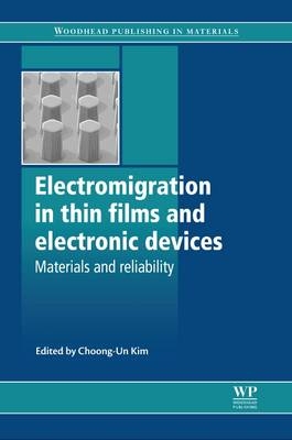
Electromigration in Thin Films and Electronic Devices
Woodhead Publishing Ltd (Verlag)
978-1-84569-937-6 (ISBN)
- Keine Verlagsinformationen verfügbar
- Artikel merken
Understanding and limiting electromigration in thin films is essential to the continued development of advanced copper interconnects for integrated circuits. Electromigration in thin films and electronic devices provides an up-to-date review of key topics in this commercially important area.
Part one consists of three introductory chapters, covering modelling of electromigration phenomena, modelling electromigration using the peridynamics approach and simulation and x-ray microbeam studies of electromigration. Part two deals with electromigration issues in copper interconnects, including x-ray microbeam analysis, voiding, microstructural evolution and electromigration failure. Finally, part three covers electromigration in solder, with chapters discussing topics such as electromigration-induced microstructural evolution and electromigration in flip-chip solder joints.
With its distinguished editor and international team of contributors, Electromigration in thin films and electronic devices is an essential reference for materials scientists and engineers in the microelectronics, packaging and interconnects industries, as well as all those with an academic research interest in the field.
Choong-Un Kim is Professor of Materials Science and Engineering at the University of Texas at Arlington, USA.
Contributor contact details
Part I: Introduction
Chapter 1: Modeling of electromigration phenomena
Abstract:
1.1 Introduction
1.2 Analytical methods
1.3 Numerical methods
1.4 Conclusion
Chapter 2: Modeling electromigration using the peridynamics approach
Abstract:
2.1 Introduction
2.2 Previous approaches to modeling electromigration (EM)
2.3 Peridynamics (PD)
2.4 PD and EM
2.5 Illustrative example
2.6 Computational requirements: present and future
2.7 Conclusions
Chapter 3: Modeling, simulation, and X-ray microbeam studies of electromigration
Abstract:
3.1 Introduction
3.2 Modeling and simulation approaches
3.3 Experimental, modeling and simulation findings
3.4 Conclusions
3.5 Acknowledgments
Part II: Electromigration in copper interconnects
Chapter 4: X-ray microbeam analysis of electromigration in copper interconnects
Abstract:
4.1 Introduction
4.2 Samples and X-ray microdiffraction methods
4.3 Electromigration (EM)-induced strains in conductor lines
4.4 Conclusions and summary
4.6 Appendix
Chapter 5: Voiding in copper interconnects during electromigration
Abstract:
5.1 Introduction
5.2 Void nucleation
5.3 Void growth
5.4 Immortality
5.5 Future trends
5.6 Acknowledgements
Chapter 6: The evolution of microstructure in copper interconnects during electromigration
Abstract:
6.1 Introduction
6.2 Copper microstructure evolution during electromigration
6.3 Plasticity and materials degradation mechanisms in copper interconnects
6.4 Implications for the reliability of advanced copper interconnect schemes
6.5 Conclusions and future trends
Chapter 7: Scaling effects on electromigration reliability of copper interconnects
Abstract:
7.1 Introduction
7.2 Mass transport during electromigration (EM)
7.3 Effect of via scaling on EM reliability
7.4 Multi-linked statistical tests for via reliability
7.5 Methods to improve the EM lifetime
7.6 Conclusion and future trends
7.7 Acknowledgements
Chapter 8: Electromigration failure in nanoscale copper interconnects
Abstract:
8.1 Process solutions being developed for copper interconnects
8.2 Electromigration (EM) scaling by generation
8.3 Suppression by metal capping: blocking rate-limiting EM pathways
8.4 Copper microstructure impact
8.5 Conclusions
8.6 Acknowledgements
Part III: Electromigration in solder
Chapter 9: Electromigration-induced microstructural evolution in lead-free and lead–tin solders
Abstract:
9.1 Introduction
9.2 Intermetallic compound formation
9.3 Void formation
9.4 Formation of whisker and hillock
9.5 Grain reorientation and grain rotation
9.6 Dissolution and recrystallization
Chapter 10: Electromigration in flip-chip solder joints
Abstract:
10.1 Introduction
10.2 Electromigration (EM)-induced voiding failure of solder interconnects
10.3 Joule heating-enhanced dissolution of under bump metallurgy (UBM) and the diffusion of on-chip metal interconnects
10.4 Stress-related degradation of solder interconnects under EM
10.5 Thermomigration (TM) behavior in solder interconnects under a thermal gradient
10.6 Conclusions
10.7 Acknowledgements
Index
| Reihe/Serie | Woodhead Publishing Series in Electronic and Optical Materials |
|---|---|
| Verlagsort | Cambridge |
| Sprache | englisch |
| Maße | 156 x 234 mm |
| Gewicht | 680 g |
| Themenwelt | Technik ► Elektrotechnik / Energietechnik |
| ISBN-10 | 1-84569-937-8 / 1845699378 |
| ISBN-13 | 978-1-84569-937-6 / 9781845699376 |
| Zustand | Neuware |
| Haben Sie eine Frage zum Produkt? |
aus dem Bereich


