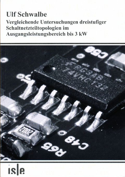
Vergleichende Untersuchungen dreistufiger Schaltnetzteiltopologien im Ausgangsleistungsbereich bis 3 kW
Seiten
2009
ISLE Steuerungstechnik und Leistungselektronik (Verlag)
978-3-938843-49-9 (ISBN)
ISLE Steuerungstechnik und Leistungselektronik (Verlag)
978-3-938843-49-9 (ISBN)
Switch mode power supplies (SMPS) are well established in our modern world. Their main
advantages are the realization of high efficiency and energy saving potential. Another benefit
and design objective is a high power density to reach lightweight systems of small size.
This thesis focuses on the benefits and the challenges of three stage DC-DC converters in
SMPS applications. They are compared to state-of-the-art two stage DC-DC converters for
high power and low output voltages. Possibilities for improvement of technical and miscellaneous
parameters should be shown.
The obtained information refers to power supply systems with maximum input power of
3680 W. This is the maximum power of a 230 V single phase supply with a 16 A fuse. The
main applications are server and telecommunication AC-DC power supplies.
Due to the complexity of SMPSs all investigations in this work have a mainly experimental
background. Theoretical descriptions and calculations would require large simplifications of
the real system. Thus, gained results would become inaccurate.
Simulations and calculations are used during the practical implementation.
Six SMPS demonstrators were developed during this dissertation work. All these systems
were designed with the same specification i.e. for 12 V output voltage and 800 W output
power. As a comparison an 800 W two stage power supply from Infineon Technologies AG
was used.
Three stage solutions can overcome the trade-offs in two stage power supplies. The optimization
problem in a two stage SMPS is to find a compromise between the bulk capacitor size
(cost) and the design of the DC-DC converter regarding the input voltage range. Three stage
power supplies use an extra stage to decouple the output power regulation from the main
stage. The main stage operates like a DC transformer. This stage can be optimized for operation
at a 100 % duty cycle. Furthermore this is a good basis for zero voltage switching (ZVS)
or resonant switching respectively. The extra stage can be implemented as a simple highly
efficient buck converter which can easily cope with the wide input voltage range.
There are two ways to arrange the buck stage. One possibility is on the primary side of the
transformer in a pre regulated concept. Here the buck converter supplies the main stage with a
constant voltage. Another possibility is an arrangement on the secondary side of the main
stage in a post regulated concept. The DC transformer stage transfers the bulk voltage with all
variations to the secondary side. The following buck stage has to maintain a constant output
voltage.
The two stage demonstrator is a voltage fed, hard switching half bridge with power factor
correction (PFC) stage.
The following pre regulated three stage powers supplies were investigated: current fed push
pull converter, current fed full bridge converter and a current fed parallel resonant converter.
The research of post regulated three stage SMPSs concentrates on: hard switching half bridge,
serial resonant converter and an LLC converter. All three stages operate with a PFC stage.
The main results of this dissertation are summarised below.
The following characteristics apply to pre regulated switch mode power supplies: The main
primary side MOSFETs in the current fed push pull converter and in the current fed full
bridge converter are stressed with high voltages. However, the secondary side rectifier MOSFETs
in all current fed systems operate with low voltage stress.
The current fed parallel resonant converter is a modification of the current fed full bridge converter
to achieve low switching losses in resonant mode operation. The stress on the active
components is analogue to the full bridge converter. A drawback of this solution is the load
dependent resonant and transfer behaviour.
The implementation of synchronous rectification control in these current fed systems needs
some effort. Self driven circuits were not sufficient.
A topology with a current fed main stage is not adequate for the generation of high currents
and low output voltages. The main reason for this is the high stress on the active components
due to the leakage inductance in the system.
Post regulated power supplies are characterised by the following facts: The investigation on
the hard switching half bridge revealed load dependent transfer behaviour. Therefore this converter
is unsuitable for a DC transformer application. Furthermore a limitation choke for the
current rise and clamping diodes was necessary to achieve ZVS and low voltage stress on the
secondary side rectifiers. Also, due to the occurring voltage drop the limitation choke reduces
the converter output power.
The serial resonant converter is suitable as a DC transformer in high output power applications.
The load current is used to charge the output capacitances of the MOSFETs to achieve
ZVS condition. The ZVS condition is lost at light load operation, influenced by the switching
frequency, interlock time and the angle of switching. If the ZVS condition is lost, the primary
MOSFETs in the resonant converter operate in hard switching mode with high switching
losses.
A modified serial resonant topology, the LLC converter, solves the problem of losing ZVS at
light load operation. ZVS condition is supported by the transformer magnetising current
which is independent of the load current. ZVS condition can be achieved over a wide operation
range to limit losses in the primary side MOSFETs. The LLC converter is a real load independent
DC transformer. This is a major result of this research.
The main advantage of a three stage solution compared to a two stage power supply is the
reduction of the bulk capacitance. The voltage variation at the bulk capacitor during a brownout
is regulated with a simple buck converter. The reduced bulk capacitance leads to cost savings
and a gain in power density. The galvanic isolation and the output regulation is separated
in a three stage concept, therefore the design of the stages is quite simple.
Every stage can operate independently, therefore the system gains degrees of freedom. More
freedom in design leads to a better adjustment between three stage SMPS and application.
If required, a synchronisation between the stages can be implemented. The load current of the
bulk capacitor can be reduced by synchronising the PFC stage and the following stage in high
power system.
Normally, the design of the different stages in a three stage SMPS is quite simple, because of
the spreading of the output power regulation and the galvanic isolation to different stages.
This separation could be used in a three stage LLC converter to reach a gain in efficiency
compared to a two stage setup.
The possibility for discrete optimisation of the stages leads to an optimised SMPS system.
The main drawback of a three stage solution is the higher component count, compared to a
two stage supply. However, higher component count and system costs do not correlate directly.
A practical comparison between the investigated power supplies showed a similar cost
level.
The major goal of the thesis, to achieve a gain in efficiency with three stage SMPSs compared
to a two stage solution, was not reached completely. The main reason is the high switching
frequency in the different stages. High switching frequency leads to high switching losses in
the switches.
At full load operation the efficiency of the three stage LLC converter was less than in the two
stage SMPS. However, at light load the situation reversed. The three stage LLC converter
reached higher efficiency than the two stage SMPS.
Due to the reduction of bulk capacitor size, an improvement of power density was reached
with three stage solutions, compared to two stage SMPSs.
This investigation highlights the qualitative properties of the different topologies. All quantitative
statements in this work refer to current state-of-the-art semiconductors and passive
components. Due to the permanent development in these fields all conclusions are only indicative.
In this research currently common switching frequencies have been proven. Therefore, the
efficiency values show not the maximum values for these topologies. A reduction of the
switching frequency would lead to a gain in total efficiency. By using state-of-the-art semiconductors
and passive components, switching frequencies of about 70 kHz to 130 kHz are
optimal for achieving high efficiency.
For high output power interleaved topologies in combination with low switching frequencies
(70 kHz to 130 kHz) are reasonable. Cancellation effects caused by control can be used to
reduce passive components stress in these topologies.
It became clear that the LLC converter with secondary side buck converter is the best three
stage solution. Due to the excellent properties in a three stage solution the combination of an
LLC converter with a primary side buck stage is reasonable, too. This setup would facilitate
the design of the buck regulator stage. This configuration could be investigated in ongoing
research. An efficiency estimation is already given in this thesis.
| Erscheint lt. Verlag | 11.12.2009 |
|---|---|
| Sprache | deutsch |
| Maße | 150 x 210 mm |
| Einbandart | Paperback |
| Themenwelt | Technik ► Elektrotechnik / Energietechnik |
| Schlagworte | 3-stage SMPS • dreistufige Schaltnetzteile • Serienresonanzkonverter • Taschenbuch / Technik/Elektronik, Elektrotechnik, Nachrichtentechnik |
| ISBN-10 | 3-938843-49-7 / 3938843497 |
| ISBN-13 | 978-3-938843-49-9 / 9783938843499 |
| Zustand | Neuware |
| Haben Sie eine Frage zum Produkt? |
Mehr entdecken
aus dem Bereich
aus dem Bereich
Kolbenmaschinen - Strömungsmaschinen - Kraftwerke
Buch | Hardcover (2023)
Hanser (Verlag)
49,99 €
