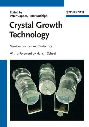
Crystal Growth Technology
Wiley-VCH (Verlag)
978-3-527-32593-1 (ISBN)
- Titel ist leider vergriffen;
keine Neuauflage - Artikel merken
Ein international zusammengesetztes Expertenteam stellt Ihnen die neuesten Aufwachsverfahren für Einkristalle vor und erklärt moderne Anwendungen in der Produktion von Halbleiterwerkstoffen und Dielektrika.
Peter Capper is a Materials Team Leader at SELEX GALILEO Infrared Ltd (formerly BAE Systems), and has over 30 years of experience in the infrared material mercury cadmium telluride (MCT). He holds the patent for the application of the accelerated crucible rotation technique to Bridgman growth and is recognised as a world authority on MCT. He has authored/co-authored over 100 Journal articles and edited/co-edited/co-written 10 books on electronic materials and devices. He has served on several International Advisory boards to conferences, acted as co-Chair at an E-MRS Symposium (France) and a SPIE Symposium (USA) and has edited/co-edited several conference proceedings for J. Crystal Growth and J. Materials Science. He is also currently on the editorial board of the Journal of Materials Science: Materials in Electronics and is a Series Editor on the Wiley Series `Materials for Electronic and Optoelectronic Appliations¿. In 2008 he received an award from the Swiss Crystallographic Society for his bulk growth work. Peter Rudolph is currently the coordinator of the technology department of the Leibniz-Institute for Crystal Growth in Berlin. His present research field is the growth of semiconductor crystals (GaAs, Ge, Si) in magnetic fields. He obtained the PhD in Solid State Physics at the Technical University of Lvov in 1972, and in 1985 the Professor position at the Humboldt University in Berlin. From 1993-94 he was Guest Professor at the Tohoku University in Sendai. He is associate editor of J. Crystal Growth, president of the German Society of Crystal Growth and member of the IOCG executive committee. He is the author of one monograph, more than 200 papers and book chapters, 7 books editions and 33 patent descriptions. He acted as co-chair and advisor of several international conferences and schools. He received innovation prizes in 2001 and 2008.
Preface
PART I: Basic Concepts in Crystal Growth Technology
THERMODYNAMIC MODELING OF CRYSTAL-GROWTH PROCESSES
Introduction
General Approach of Thermodynamic Modeling
Crystal Growth in the System Si-C-O-Ar (Example 1)
Crystal Growth of Carbon-Doped GaAs (Example 2)
Summary and Conclusions
MODELING OF VAPOR-PHASE GROWTH OF SiC AND AlN BULK CRYSTALS
Introduction
Model Description
Results and Discussions
Conclusions
ADVANCED TECHNOLOGIES OF CRYSTAL GROWTH FROM MELT USING VIBRATIONAL INFLUENCE
Introduction
Axial Vibrational Control in Crystal Growth
AVC-Assisted Czochralski Method
AVC-Assisted Bridgman Method
AVC-Assisted Floating Zone Method
Conclusions
PART II: Semiconductors
NUMERICAL ANALYSIS OF SELECTED PROCESSES IN DIRECTIONAL SOLIDIFICATION OF SILICON FOR PHOTOVOLTAICS
Introduction
Directional Solidification Method
Crystallization Process
Impurity Incorporation in Crystals
Summary
CHARACTERIZATION AND CONTROL OF DEFECTS IN VCz GaAs CRYSTALS GROWN WITHOUT B2O3 ENCAPSULANT
Introduction
Retrospection
Crystal Growth Without B2O3 Encapsulant
Inclusions, Precipitates and Dislocations
Residual Impurities and Special Defect Studies
Electrical and Optical Properties in SI GaAs
Boron in SC GaAs
Outlook on TMF-VCz
Conclusions
THE GROWTH OF SEMICONDUCTOR CRYSTALS (Ge, GaAs) BY THE COMBINED HEATER MAGNET TECHNOLOGY
Introduction
Selected Fundamentsals
TMF Generation in Heater-Magnet Modules
The HMM Design
Numerical Measurements
Growth Results under TMF
Conclusions and Outlook
MANUFACTURING OF BULK AlN SUBSTRATES
Introduction
Modeling
Experiment
Results and Discussion
Conclusions
INTERACTIONS OF DISLOCATIONS DURING EPITAXIAL GROWTH OF SiC AND GaN
Introduction
Classification, Nomenclature and Characterization of Dislocations in SiC and GaN
Conversion of Basal Plane Dislocations During SiC Epitaxy
Reduction of Dislocations During Homoepitaxy of GaN
Conclusions
LOW-TEMPERATURE GROWTH OF TERNARY III-V SEMICONDUCTOR CRYSTALS FROM ANTIMONIDE-BASED QUATERNARY MELTS
Introduction
Crystal Growth from Quaternary Melts
Synthesis and Bulk Crystal Growth
Conclusion
MERCURY CADMIUM TELLURIDE (MCT) GROWTH TECHNOLOGY USING ACRT AND LPE
Introduction
Bridgman/ACRT Growth of MCT
Liquid Phase Epitaxy of MCT
THE USE OF A PLATINUM TUBE AS AN AMPOULE SUPPORT IN THE BRIDGMAN GROWTH OF BULK CZT CRYSTALS
Introduction
The Importance of the Solid/Liquid Interface
Approaches for Crystal Growth Using Ampoule Support
Results and Discussions
Conclusions
PART III: Dielectrics
MODELING AND OPTIMIZATION OF OXIDE CRYSTAL GROWTH
Introduction
Radiative Heat Transfer (RHT)
Numerical Model
Results and Discussion
Conclusions
ADVANCED MATERIAL DEVELOPMENT FOR INERTIAL FUSION ENERGY (IFE)
Introduction
Production of Nd:Phosphate Laser Glass and KDP Frequency-Conversion Crystals
Yb:S-FAP Crystals
YCOB Crystals
Advanced Material Concepts for Power-Plant Designs
Summary
MAGNETO-OPTIC GARNET SENSOR FILMS: PREPARATION, CHARACTERIZATION, APPLICATION
Introduction
Bi-Substituted Garnets
LPE Deposition and Topological Film Properties
Applications
Conclusions
GROWTH TECHNOLOGY AND LASER PROPERTIES OF Yb-DOPED SESQUIOXIDES
Introduction
Structure and Physical Properties
Crystal Growth
Spectroscopic Characterization
Laser Experiments
Summary and Outlook
CONTINUOUS GROWTH OF ALKALI-HALIDES: PHYSICS AND TECHNOLOGY
Modern Requirements to Large Alkali-Halide Crystals
Conditions of Steady-State Crystallization in Conventional Melt-Growth Methods and in Their Modifications
Macrodefect Formation in AHC
Dynamics of Thermal Conditions during Continuous Growth
Advanced Growth-Control Algorithms
Summary
TRENDS IN SCINTILLATION CRYSTALS
Introduction
Novel Scintillation Materials
Scintillation Detectors for Image Visualization and Growth Techniques for Scintillation Crystals
High Spatial Resolution Scintillation Detectors
Conclusions
PART IV: Crystal Machining
CRYSTAL MACHINING USING ATMOSPHERIC PRESSURE PLASMA
Introduction
Plasma Chemical Vaporization Machining (PCVM)
Numerically Controlled Sacrificial Oxidation
Conclusions
"Edited by the organizers of the International Workshop on Crystal Growth Technology, this ready reference is essential reading for materials scientists, chemists, physicists, computer hardware manufacturers, engineers, and those working in the chemical and semiconductor industries." (Quote.com, 31 January 2011)
"Semiconductors and dielectrics are two essential materials found in cell phones and computers, for example, and both are manufactured by growing crystals." (Quote.com, 20 January 2011)
| Erscheint lt. Verlag | 25.8.2010 |
|---|---|
| Vorwort | Hans J. Scheel |
| Sprache | englisch |
| Maße | 170 x 240 mm |
| Gewicht | 930 g |
| Themenwelt | Technik ► Elektrotechnik / Energietechnik |
| Schlagworte | chemical engineering • Chemie • Chemische Verfahrenstechnik • Chemistry • Component Manufacturing • Dielektrikum • Dielektrizität • Electrical & Electronics Engineering • Electrical & Electronics Engineering • Elektrotechnik u. Elektronik • Halbleiter • Halbleiterphysik • Komponentenfertigung • Kristalle • Kristallzüchtung • Physical Chemistry • Physics • Physik • Physikalische Chemie • Semiconductor physics • semiconductors |
| ISBN-10 | 3-527-32593-X / 352732593X |
| ISBN-13 | 978-3-527-32593-1 / 9783527325931 |
| Zustand | Neuware |
| Haben Sie eine Frage zum Produkt? |
aus dem Bereich
