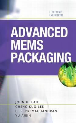
Advanced MEMS Packaging
McGraw-Hill Professional (Verlag)
978-0-07-162623-1 (ISBN)
- Titel z.Zt. nicht lieferbar
- Versandkostenfrei innerhalb Deutschlands
- Auch auf Rechnung
- Verfügbarkeit in der Filiale vor Ort prüfen
- Artikel merken
Publisher's Note: Products purchased from Third Party sellers are not guaranteed by the publisher for quality, authenticity, or access to any online entitlements included with the product.
A comprehensive guide to 3D MEMS packaging methods and solutionsWritten by experts in the field, Advanced MEMS Packaging serves as a valuable reference for those faced with the challenges created by the ever-increasing interest in MEMS devices and packaging. This authoritative guide presents cutting-edge MEMS (microelectromechanical systems) packaging techniques, such as low-temperature C2W and W2W bonding and 3D packaging.
This definitive resource helps you select reliable, creative, high-performance, robust, and cost-effective packaging techniques for MEMS devices. The book will also aid in stimulating further research and development in electrical, optical, mechanical, and thermal designs as well as materials, processes, manufacturing, testing, and reliability. Among the topics explored:
Advanced IC and MEMS packaging trends
MEMS devices, commercial applications, and markets
More than 360 MEMS packaging patents and 10 3D MEMS packaging designs
TSV for 3D MEMS packaging
MEMS wafer thinning, dicing, and handling
Low-temperature C2C, C2W, and W2W bonding
Reliability of RoHS-compliant MEMS packaging
Micromachining and water bonding techniques
Actuation mechanisms and integrated micromachining
Bubble switch, optical switch, and VOA MEMS packaging
Bolometer and accelerameter MEMS packaging
Bio-MEMS and biosensor MEMS packaging
RF MEMS switches, tunable circuits, and packaging
John H. Lau received his Ph.D. degree in Theoretical and Applied Mechanics from the University of Illinois (1977), a M.A.Sc. degree in Structural Engineering from the University of British Columbia (1973), a second M.S. degree in Engineering Physics from the University of Wisconsin (1974), and a third M.S. degree in Management Science from Fairleigh Dickinson University (1981). He also has a B.E. degree in Civil Engineering from National Taiwan University (1970). John is an interconnection technology scientist at Agilent Technologies, Inc. His current interests cover a broad range of electronic and optoelectronic packaging and manufacturing technology. Prior to Agilent, he worked for Express Packaging Systems, Hewlett-Packard Company, Sandia National Laboratory, Bechtel Power Corporation, and Exxon Production and Research Company. With more than 30 years of R&D and manufacturing experience in the electronics, petroleum, nuclear, and defense industries, he has given over 200 workshops, authored and co-authored over 180 peer reviewed technical publications, and is the author and editor of 13 books: Solder Joint Reliability; Handbook of Tape Automated Bonding; Thermal Stress and Strain in Microelectronics Packaging; The Mechanics of Solder Alloy Interconnects; Handbook of Fine Pitch Surface Mount Technology; Chip On Board Technologies for Multichip Modules; Ball Grid Array Technology; Flip Chip Technologies; Solder Joint Reliability of BGA, CSP, Flip Chip, and Fine Pitch SMT Assemblies; Electronics Packaging: Design, Materials, Process, and Reliability; Chip Scale Package (CSP): Design, Materials, Process, Reliability, and Applications; Low Cost Flip Chip Technologies for DCA, WLCSP, and PBGA Assemblies, and Microvias for Low Cost, High Density Interconnects. John served as one of the associate editors of the IEEE Transactions on Components, Packaging, and Manufacturing Technology and ASME Transactions, Journal of Electronic Packaging. He also served as general chairman, program chairman, and session chairman, and invited speaker of several IEEE, ASME, ASM, MRS, IMAPS, SEMI, and SMI International conferences. He received a few awards from ASME and IEEE for best papers and outstanding technical achievements, and is an ASME Fellow and an IEEE Fellow. He is listed in American Men and Women of Science and Whos Who in America.
Chapter 1 Introduction to MEMS
1.1 Introduction
1.2 Commercial Applications of MEMS
1.3 MEMS Markets
1.4 Top 30 MEMS Suppliers
1.5 Introduction to MEMS Packaging
1.6 MEMS Packaging Patents Since 2001
1.6.1 US MEMS Packaging Patents
1.6.2 Japan MEMS Packaging Patents
1.6.3 Worldwide MEMS Packaging Patents
1.7 References
Chapter 2 Advanced MEMS Packaging
2.1 Introduction
2.2 Advanced IC Packaging
2.2.1 Moore’s Law vs. More Than Moore
2.2.2 3D IC Integration and WLP
2.2.3 Low-Cost Solder Microbumps for 3D IC SiP
2.2.4 Thermal Management of 3D IC SiP with TSV
2.3 Advanced MEMS Packaging
2.3.1 3D MEMS WLP – Designs and Materials
2.3.2 3D MEMS WLP – Processes
2.4 References
Chapter 3 Enabling Technologies for Advanced MEMS Packaging
3.1 Introduction
3.2 TSV for MEMS Packaging
3.2.1 Via formations
3.2.2 Dielectric Isolation Layer (SiO2) Deposition
3.2.3 Barrier/Adhesion and Seed Metal Layer Deposition
3.2.4 Via Filling
3.2.5 Cu polishing by Chemical/Mechanical polish (CMP)
3.2.6 Fabrication of ASIC Wafer with TSV
3.2.7 Fabrication of Cap Wafer with TSV and Cavity
3.3 Piezoresistive Stress Sensors for MEMS Packaging
3.3.1 Design and Fabrication of Piezoresistive Stress Sensors
3.3.2 Calibration of Stress Sensors
3.3.3 Stresses in Wafers After Mounting on a Dicing Tape
3.3.4 Stresses in Wafers After Thinning (Back-Grinding)
3.4 MEMS Wafer Thinning and Thin-Wafer Handling
3.4.1 3M Wafer Support System
3.4.2 EV Group’s Temporary Bonding and DeBonding System
3.4.3 A Simple Support-Wafer Method for Thin Wafer Handling
3.5 Low-Temperature Bonding for MEMS Packaging
3.5.1 How Does Low Temperature Bonding with Solders Work?
3.5.2 Low Temperature C2C Bonding
2.5.3 Low Temperature C2W Bonding
2.5.4 Low Temperature W2W Bonding
3.6 MEMS Wafer Dicing
3.6.1 Fundamentals of Stealth Dicing (SD) Technology
3.6.2 Dicing of SOI Wafers
3.6.3 Dicing of Silicon-on-Silicon Wafers
3.6.4 Dicing of Silicon-on-Glass Wafers
3.7 RoHS Compliant MEMS Packaging
3.7.1 EU RoHS
3.7.2 What is the Definition of X-free, e.g., Pb-free?
3.7.3 What is a Homogeneous Material?
3.7.4 What is the TAC?
3.7.5 How a Law is Published in EU RoHS?
3.7.6 EU RoHS Exemptions
3.7.7 Current Status of RoHS Compliance in the Electronics Industry
3.7.8 Lead-Free Solder Joint Reliability of MEMS Packages
3.8 References
Chapter 4 Advanced MEMS Wafer Level Packaging
4.1 Introduction
4.2 Micromachining, Wafer Bonding Technologies and Interconnects
4.2.1 Thin Film Technologies
4.2.2 Bulk Micromachining Technologies
4.2.3 Conventional Wafer Bonding Technologies for Packaging
4.2.4 Plasma Assisted Wafer Bonding Technology
4.2.5 Electrical Interconnects
4.2.6 Solder Based Intermediate Layer Wafer Bonding Technology
4. 3 Wafer Level Encapsulation
4.3.1 High Temperature Encapsulation Process
4.3.2 Low Temperature Encapsulation Process
4. 4 Wafer Level Chip Capping and MCM Technologies
4. 5 Wafer Level MEMS Packaging Based on Low Temperature Solders – Case Study
4.5.1 Case study – In/Ag system of non-eutectic composition
4.5.2 Case study – Eutectic InSn solder for Cu/Ni/Au based metallization
4.6 Summary and Future Outlooks
4.7 References
Chapter 5 Optical MEMS Packaging - Communications
5.1 Introduction
5.2 Actuation Mechanisms and Integrated Micromachining Processes
5.2.1 Electrostatic Actuation
5.2.2 Thermal Actuation
5.2.3 Magnetic Actuation
5.2.4 Piezoelectric Actuation
5.2.5 Integrated Micromachining Processes
5.3 Optical Switches
5.3.1 Small Scale Optical Switches
5.3.2 Large Scale Optical Switches
5.4 Variable Optical Attenuators
5.4.1 Early Development Works
5.4.2 Surface Micromachined VOAs
5.4.3 DRIE Derived Planar VOAs Using Electrostatic Actuators
5.4.4 DRIE Derived Planar VOAs Using Electrothermal (Thermal) Actuators
5.4.5 3-D VOAs
5.4.6 VOAs Using Various Mechanisms
5.5 Packaging, Testing and Reliability Issues
5.5.1 Manufacturability and Self-assembly
5.5.2 Case Study – VOAs
5.5.3 Case Study – Optical Switches
5.6 Summary and Future Outlooks
5.7 References
Chapter 6 Optical MEMS Packaging - Bubble Switch
6.1 Introduction
6.2 3D Optical MEMS Packaging
6.3 Boundary Value Problem
6.3.1 Geometry
6.3.2 Materials
6.3.3 Loading Conditions
6.4 Nonlinear Analyses of the 3D Photonic Switch
6.4.1 Creep Hysteresis Loops
6.4.2 Deflections
6.4.3 Shear Stress Time-History
6.4.4 Shear Creep Strain Time-History
6.4.5 Creep Strain Energy Density Range
6.5 Isothermal Fatigue Tests and Results
6.5.1 Sample Preparation
6.5.2 Test Set-Up and Procedures
6.5.3 Test Results
6.6 Thermal-Fatigue Life Prediction of the Sealing Ring
6.7 Summary
6.8 Appendix A: Package Deflection by Twyman-Green Interferometry Method
6.9.1 Sample Preparation
6.9.2 Test Setup and Procedure
6.9.3 Temperature Conditions
6.9.4 Measurement Results
6.9 Appendix B: Package Deflection by Finite Element Method
6.10 Appendix C: Finite Element Modeling of the Bolt
6.11.1 Description of Bolted Model
6.11.2 Responses of Bolted Photonic Switch
6.11 References
Chapter 7 Bolometer MEMS Packaging
7.1 Introduction
7.2 Bolometer chip
7.3 Thermal optimization
7.3.1 Final temperature stability testing
7.4 Structural optimization of package
7.5 Vacuum packaging of Bolometer
7.5.1 Ge Window
7.6 Getter attachment and activation
7.7 Outgassing study in a Vacuum package
7.8 Testing set up for Bolometer
7.9 Image testing
7.10 References
Chapter 8: Bio MEMS Packaging
8.1 Introduction
8.2 BioMEMS chip
8.3 Micro fluidic components
8.3.1 Micro fluidic cartridge
8.3.2 Biocompatible polymeric materials
8.4 Microfluidic Packaging
8.4.1 Polymer microfabrication techniques
8.4.2 Replication technologies
8.4.3 Overview of existing DNA and RNA extractor bio-cartridges
8.5 Fabrication of PDMS layers
8.6 Assembly of PDMS microfluidic packages
8.6.1 Microfluidic package with out reservoirs
8.6.2 Development of Reservoir and Valve
8.7 Self contained Micro fluidic cartridge
8.7.1 Micro fluidic package with self contained reservoirs
8.7.2 Reservoir design for controlled fluid flow
8.7.3 Pin valve design
8.7.4 Fluid Flow control Mechanism
8.8 Fabrication
8.8.1. Substrate fabrication
8.8.2. Material selection for the reservoir membrane
8.9 Permeability of material
8.10 Thermo Compression Bonding
8.10.1 Bonding of PMMA to PMMA for Channel layer
8.10.2 Polypropylene to PMMA for Reservoir and channel layer
8.10.3 Tensile Test
8.11 Microfluidic Package Testing
8.11.1 Fluidic testing
8.11.2 Biological Testing on bio-sample
8.12 Sample Preparation and Set Up
8.12.1 Pre treatment of the cartridge
8.12.2 DNA Extraction
8.12.3 PCR amplification
8.13 References
Chapter 9 Bio Sensor MEMS Packaging
9.1 Introduction
9.1.1 Review of Optical Coherence Tomography
9.2 Biosensor packaging
9.2.1 Upper Substrate
9.2.2 Single Mode Optical Fiber and Graded Index Lens
9.2.3 Lower Substrate
9.2.4 Micro Mirror
9.3 The Package
9.3.1 The Configuration of the Probe
9.3.2 Optical Properties and Theories
9.3.3 Evaluations of Parameters
9.4 Optical Simulation
9.4.1 Optical model of the Probe
9.4.2 Effect of Mirror Curvature to Coupling Efficiency
9.4.3 Effect of Lateral Tilt in Flat Micro Mirror on a Curved Sample
9.4.4 Effect of Vertical Tilt in Flat Micro Mirror on a Curved Sample
9.4.5 Effect of Vertical Tilt in Flat Micro Mirror on a Flat Sample
9.5 Assembly of Optical probe
9.5.1 Fabrication of SiOB
9.5.2 Probe Assembly
9.5.3 Probe Housing
9.6 Testing of the Probe
9.6.1 Optical Alignment
9.6.2Axial Scanning Test Result
9.6.3 Probe imaging
9.6.4 Optical Efficiency Testing
9.7 References
Chapter 10 Accelerometer MEMS Packaging
10.1 Introduction
10.2 Wafer level package requirements
10.2.1 Electrical modeling
10.2.2 Package structure
10.2.3 Extraction methodology of the interconnection characteristics
10.3 Wafer level packaging Process
10.4 Wafer Separation Process
10.4.1 Process Integration
10.5 Sacrificial wafer removal process
10.6 Wafer level vacuum sealing
10.7 Vacuum measurement using MEMS motion analyzer (MMA)
10.8 Reliability Testing – Vacuum maintenance
10.9 Wafer level 3D package for Accelerometer
10.10 References
Chapter 11 RF MEMS Switches
11.1 Introduction
11.2 Design of RF MEMS Switches
11.2.1Electromagnetic modelling of capacitive switches
11.2.2Electromagnetic modelling of metal-contact switches
11.2.3Mechanical design of RF MEMS switches
11.3 Fabrication of RF MEMS Switches
11.3.1Surface micromachining of RF MEMS switches
11.3.2Bulk micromachining of RF MEMS switches
11.4 Characterization of RF MEMS switches
11.4.1RF performance
11.4.2Mechanical performance
11.5 Reliability of RF MEMS Switch
11.5.1Reliability of capacitive switches
11.5.2Reliability of metal-contact switches
11.6 Power Handling of RF MEMS Switches
11.6.1Power handling of capacitive switches
11.6.2Power handling of metal-contact switches
11.7 Summary
11.8 References
Chapter 12 RF MEMS Tunable Circuits
12.1 Introduction
12.2 RF MEMS Tunable Capacitors
12.2.1Analog tuning of RF MEMS capacitors
12.2.2Digital tuning of RF MEMS capacitors
12.3 RF MEMS Tunable Band-Pass Filters
12.3.1Analog tuning of RF MEMS band-pass filters
12.3.2Digital tuning of RF MEMS
band-pass filters
12.4 Summary
12.5 References
Chapter 13 Advanced Packaging of RF MEMS
13.1 Introduction
13.2 Zero-Level Packaging
13.2.1Chip capping
13.2.2Thin film capping
13.3 First–Level Packaging
13.4 Reliability of Packaged RF MEMS Devices
13.5 Summary
13.6 References
| Erscheint lt. Verlag | 16.12.2009 |
|---|---|
| Zusatzinfo | 70 Illustrations, unspecified |
| Sprache | englisch |
| Maße | 163 x 236 mm |
| Gewicht | 938 g |
| Themenwelt | Technik ► Elektrotechnik / Energietechnik |
| ISBN-10 | 0-07-162623-9 / 0071626239 |
| ISBN-13 | 978-0-07-162623-1 / 9780071626231 |
| Zustand | Neuware |
| Haben Sie eine Frage zum Produkt? |
aus dem Bereich


