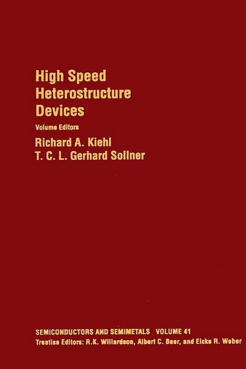
High Speed Heterostructure Devices (eBook)
454 Seiten
Elsevier Science (Verlag)
978-0-08-086438-9 (ISBN)
Key Features
* The first complete review of InP-based HFETs and complementary HFETs, which promise very low power and high speed
* Offers a complete, three-chapter review of resonant tunneling
* Provides an emphasis on circuits as well as devices
Volume 41 includes an in-depth review of the most important, high-speed switches made with heterojunction technology. This volume is aimed at the graduate student or working researcher who needs a broad overview andan introduction to current literature. - The first complete review of InP-based HFETs and complementary HFETs, which promise very low power and high speed- Offers a complete, three-chapter review of resonant tunneling- Provides an emphasis on circuits as well as devices
Front Cover 1
High Speed Heterostructure Devices 4
Copyright Page 5
Contents 6
List of Contributors 10
Preface 12
Chapter 1. Quantum Electron Devices: Physics and Applications 14
I. Introduction 15
II. Resontant-Tunneling Diodes 17
III. Resonant Tunneling Bipolar Transistors (RTBTs) with Double Barrier in the Base 37
IV. Devices with Multiple-Peak I–V Characteristics and Multiple-State RTBTs 46
V. Circuit Applications 54
VI. Unipolar Resonant Tunneling Transistors 62
VII. Superlattice Transport and Quantum Reflections 69
VIII. Field-Induced Localization in Vertical and Parallel Transport 74
Acknowledgments 87
References 87
Chapter 2. GaAs–Gate Semiconductor–Insulator–Semiconductor FET 92
I. Introduction—Basic Principles 93
II. History and Development of SISFETs and Related Devices 96
III. SIS Capacitors 101
IV. Design of Vertical Structure 110
V. Processing Issues 123
VI. FET Characteristics 130
VII. SISFET Modeling 147
VIII. Circuit Results 159
IX. Discussion and Future Perspective 164
Acknowledgments 166
References 166
Chapter 3. Unipolar InP-Based Transistors 170
I. Introduction 170
II. Growth of InP-Based Structures 175
III. InP Field Effect Transistors (FETs) 180
IV. High Electron Mobility Transistors (HEMTs) 186
V. Summary 225
VI. Acknowledgments 226
References 226
Chapter 4. Complementary Heterostructure FET Integrated Circuits 232
I. Introduction 233
II. Circuit Issues 234
III. Materials 243
IV. Heterostructure Transport 247
V. Heterostructure Device Design 268
VI. Integration 274
VII. Fabrication 279
VIII. Device Characteristics and Circuit Performance 288
IX. Concluding Remarks 298
Acknowledgments 298
References 299
Chapter 5. GaAs-Based and InP-Based Heterostructure Bipolar Transistors 304
I. Introduction 305
II. Current Gain and Some Key Electrical Properties in HBT Designs 308
III. Epitaxial Growth of HBT Structures 317
IV. Device Fabrication Process and Related Issues 330
V. Nonequilibrium Electron Transport in HBTs 341
VI. Device Characteristics and Limiting Factors 350
VII. Implementation of HBTs in Integrated Circuits 362
VIII. Summary and Prospects 365
References 367
Chapter 6. High-Frequency Resonant-Tunneling Devices 372
I. Introduction 372
II. Times in Resonant Tunneling 381
III. High-Frequency Applications 400
IV. Future Expectations 423
Acknowledgments 424
References 425
List of Variables 430
Chapter 7. Resonant-Tunneling Hot-Electron Transistors and Circuits 434
I. Introduction 434
II. Hot Electron Transport in RHETs 435
III. RHET dc and Microwave Characteristics 443
IV. RHET Circuit Applications 449
V. RHET Room-Temperature Operation 456
VI. Summary 459
Acknowledgment 459
References 459
Index 462
Contents of Volumes in This Series 468
GaAS-Gate Semiconductor–Insulator–Semiconductor FET
Paul Solomon; David J. Frank; Steven L. Wright; Frank Canora IBM Research Dmsion, IBM T. J. Watson Research Center YorkTown Heights, New York
I Introduction—Basic Principles
The SISFET or “GaAs gate FET,” as it was originally called, belongs to an extensive family of heterojunction field effect transistors (Tiwari, 1992; Sze, 1990; Solomon and Morkoç, 1984) built out of III–V compounds, and known collectively as HFETs. These FETs are characterized by high electron mobilities and transport velocities for electrons in the channel formed at the heterojunction boundary between two semiconductors having different electron affinities. As a result, these HFETs achieve high speeds in both digital and analog (microwave) applications and low-noise operation as microwave amplifiers.
It is primarily in analog applications that HFETs have achieved commercial success to date, although the conventional GaAs MESFET (metal semiconductor FET) has begun to penetrate the digital market (e.g., the CONVEX [McDonald, 1991] and CRAY [Kiefer et al., 1987; Wilson et al., 1991] supercomputers). If the digital market becomes established, HFETs would provide for the following generations. The SISFET is intended primarily for digital applications.
The first HFETs were modulation doped FETs (MODFETs) where the wider bandgap semiconductor (AlGaAs) was doped, and electrons spilled over into the narrow bandgap semiconductor (GaAs) forming a channel there. Because of the confinement of the electrons in this channel, coupled with the low effective mass of GaAs, the perpendicular momenta of the electrons in the channel are quantized, with appreciable effects even at room temperature, so that this channel is often referred to as a twodimensional electron gas (2DEG).
With molecular beam epitaxy capable of growing wide bandgap AlGaAs layers on GaAs, with sharp interfaces, the AlGaAs could be used as the gate insulator of an FET. As was pointed out by Solomon (1982a), the existence of an appropriate field boundary condition at the GaAs/AlGaAs interface such that the 2DEG satisfies Gauss’s law
Nch=εFch,
(1)
where Nch is the sheet electron concentration, ε the permittivity of GaAs and Fch the field in the GaAs at the GaAs/AlGaAs interface (the field in the bulk GaAs is assumed to be zero). This field can be supplied either by doping in the AlGaAs, as in a MODFET or, as in a conventional Si MOSFET, by an applied gate voltage. Looked at another way, the doping in a MODFET is equivalent to charge in the insulator of a MOSFET.
The SISFET or GaAs gate FET (Solomon et al., 1984; Matsumoto et al., 1984) was derived as an analog of the polysilicon gate MOSFET, where the n+ GaAs, i AlGaAs, and i or p− GaAs of the SISFET replace the n+ polysilicon, SiO2 and p silicon of the MOSFET. The comparison between the devices is illustrated in Fig. 1. The main advantages of the SISFET over the MOSFET are the better electron transport properties in the channel, and the fact that the entire vertical structure is a single crystal, eliminating many problems pertaining to interface charge and interface states that can affect MOSFETs. The major disadvantage of this structure is the low barrier height of the gate “insulator” (0.35 eV at most for GaAs/AlGaAs), which compares unfavorably with ~3 eV for Si/SiO2. This means that gate leakage currents are much higher in SISFETs than in MOSFETs. The positive aspect of this is that there are no long-term charge trapping effects in the AlGaAs, at least down to 77 K, like those that have plagued the MOSFET.
Band diagrams of the SISFET and the MODFET are compared in Fig. 2. The main differences are the replacement of doped with undoped AlGaAs, and the replacement of the gate Schottky barrier with a heterojunction barrier. The threshold voltage for either device may be written as
T=Φg−Φch−eNIt122ε1+εεIFBtI,
(2)
where εI, tI and NI are the permittivity, thickness and doping of the gate insulator, Φg and Φch the barrier heights (measured from the quasi-Fermi levels when biased at threshold) at the gate and channel interfaces, and FB the back field originating from behind the channel due to doping, trapped charge, etc. (see Section IV.D for more details).
This equation yields the zero threshold voltage property of the SISFET when NI ≈ 0, and for small back fields, due to the fact that Φg ≈ Φch for the same material in gate and channel. This property is independent of the thickness of the AlGaAs. For use in digital circuits, it is necessary to adjust VT to a small, positive value, and several ways to do this will be discussed. Furthermore, it is necessary to adjust the threshold voltage differently for enhancement- and depletion-mode FETs, necessitating the use of doping in at least one of them. In addition, uncontrolled doping and trapped charge in the barrier or substrate will cause threshold voltage shifts. Given this, the SISFET still retains superior threshold control properties compared to MODFETs or MESFETs. In the MODFET, for example, VT is extremely sensitive to doping and thickness, because of the large difference between Φg and Φch. Tolerances of doping of ~2% and thicknesses of ~1% are required for the MODFET to meet the stringent VT control requirements of digital logic.
Doping of the AlGaAs has introduced another problem for MODFETs, from which the SISFET escapes. Every donor in the AlGaAs can potentially become a deep electron trap when it captures an electron, through a process of lattice deformation. These “DX” centers (Mooney, 1990) have been the bane of MODFETs and have forced MODFET designers to use low AlAs mole fractions (~25%), resulting in poor electron confinement by the heterobarrier. In contrast to this, the SISFET can use a high AlAs mole fraction (~50%) optimized for low leakage current.
This chapter will discuss the SISFET, mainly using examples from IBM’s SISFET program. A review of this work has been given recently (Kiehl et al., 1990), although the present review will be much more detailed in its treatment of device and circuit designs, as well as presenting previously unpublished device and circuit results of the present authors. Much has been learned from this program about SISFETs, and about FET III–V HFETs in general. Looking toward the future, this chapter concludes that the scalability of SISFETs to gate lengths smaller than 14μm will require semiconductor pairs having higher barrier heights than can be obtained with GaAs/AlGaAs. This may be fulfilled by InGaAs and InAlAs.
II History and Development of SISFETs and Related Devices
The family of SISFETs and related devices include the SISFET itself, in both GaAs-gate and Ge-gate implementations; some version of the MISFET; and the doped channel MISFET. Often different acronyms are used by different groups of researchers. All of these devices have the common feature that the gate insulator is an undoped, wide-bandgap, III–V semiconductor. These FETs have also been used for complementary heterostructure logic, which is discussed in a separate chapter of this book entitled “Complementary Heterostructure FET Integrated Circuits,” by Kiehl, and the reader is referred there for details not covered in what follows.
A CONCEPT AND FIRST REALIZATION
The concept of the SISFET as a close analog of the MOSFET was first put forward by Rosenberg (1986). Solomon (1982b) realized the advantages of the zero threshold voltage property of the SISFET and came up with an independent proposal.
The properties of GaAs/AlGaAs/GaAs SIS capacitors consisting of n+ GaAs − i Al0.4Ga0.6As − n GaAs were then investigated, by Solomon and Hickmott (1983), in much the same way as MOS capacitors, to study the charge control properties and gate leakage current characteristics of the basic vertical structure. The results show MOS-like CV curves (Fig. 3) and IV characteristics (Fig. 4) that reveal the basic leakage current mechanisms of thermionic emission at high temperature and Fowler-Nordheim tunneling at low temperature. The GaAs/AlGaAs interface was capable of supporting electron densities of greater than...
| Erscheint lt. Verlag | 6.7.1994 |
|---|---|
| Mitarbeit |
Herausgeber (Serie): Albert C. Beer, Eicke R. Weber |
| Sprache | englisch |
| Themenwelt | Schulbuch / Wörterbuch |
| Naturwissenschaften ► Physik / Astronomie ► Elektrodynamik | |
| Naturwissenschaften ► Physik / Astronomie ► Festkörperphysik | |
| Technik ► Elektrotechnik / Energietechnik | |
| Technik ► Maschinenbau | |
| ISBN-10 | 0-08-086438-4 / 0080864384 |
| ISBN-13 | 978-0-08-086438-9 / 9780080864389 |
| Informationen gemäß Produktsicherheitsverordnung (GPSR) | |
| Haben Sie eine Frage zum Produkt? |
Kopierschutz: Adobe-DRM
Adobe-DRM ist ein Kopierschutz, der das eBook vor Mißbrauch schützen soll. Dabei wird das eBook bereits beim Download auf Ihre persönliche Adobe-ID autorisiert. Lesen können Sie das eBook dann nur auf den Geräten, welche ebenfalls auf Ihre Adobe-ID registriert sind.
Details zum Adobe-DRM
Dateiformat: EPUB (Electronic Publication)
EPUB ist ein offener Standard für eBooks und eignet sich besonders zur Darstellung von Belletristik und Sachbüchern. Der Fließtext wird dynamisch an die Display- und Schriftgröße angepasst. Auch für mobile Lesegeräte ist EPUB daher gut geeignet.
Systemvoraussetzungen:
PC/Mac: Mit einem PC oder Mac können Sie dieses eBook lesen. Sie benötigen eine
eReader: Dieses eBook kann mit (fast) allen eBook-Readern gelesen werden. Mit dem amazon-Kindle ist es aber nicht kompatibel.
Smartphone/Tablet: Egal ob Apple oder Android, dieses eBook können Sie lesen. Sie benötigen eine
Geräteliste und zusätzliche Hinweise
Buying eBooks from abroad
For tax law reasons we can sell eBooks just within Germany and Switzerland. Regrettably we cannot fulfill eBook-orders from other countries.
aus dem Bereich


