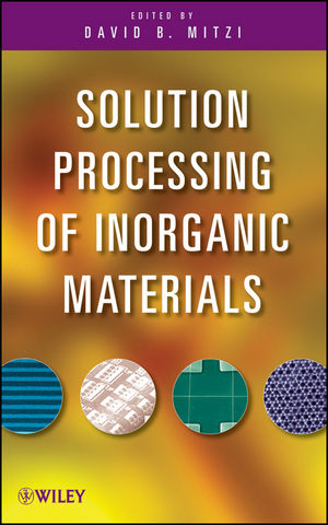
Solution Processing of Inorganic Materials
Wiley-Interscience (Verlag)
978-0-470-40665-6 (ISBN)
Discover the materials set to revolutionize the electronics industry
The search for electronic materials that can be cheaply solution-processed into films, while simultaneously providing quality device characteristics, represents a major challenge for materials scientists. Continuous semiconducting thin films with large carrier mobilities are particularly desirable for high-speed microelectronic applications, potentially providing new opportunities for the development of low-cost, large-area, flexible computing devices, displays, sensors, and solar cells.
To date, the majority of solution-processing research has focused on molecular and polymeric organic films. In contrast, this book reviews recent achievements in the search for solution-processed inorganic semiconductors and other critical electronic components. These components offer the potential for better performance and more robust thermal and mechanical stability than comparable organic-based systems.
Solution Processing of Inorganic Materials covers everything from the more traditional fields of sol-gel processing and chemical bath deposition to the cutting-edge use of nanomaterials in thin-film deposition. In particular, the book focuses on materials and techniques that are compatible with high-throughput, low-cost, and low-temperature deposition processes such as spin coating, dip coating, printing, and stamping. Throughout the text, illustrations and examples of applications are provided to help the reader fully appreciate the concepts and opportunities involved in this exciting field.
In addition to presenting the state-of-the-art research, the book offers extensive background material. As a result, any researcher involved or interested in electronic device fabrication can turn to this book to become fully versed in the solution-processed inorganic materials that are set to revolutionize the electronics industry.
David B. Mitzi, PhD, is a Research Staff Member in the Physical Sciences Department at the IBM Thomas J. Watson Research Center. His research examines the solid-state chemistry, thin-film deposition and device opportunities for a variety of materials with potentially useful electronic or optical properties. Most recently, his focus has been on organic-inorganic hybrids and the development of solution-processed high-mobility inorganic semiconductors for thin-film devices (e.g., TFTs, LEDs, solar cells). Dr. Mitzi holds a number of patents and has authored or coauthored more than one hundred papers.
Preface. Contributors.
1. Introduction to Solution-Deposited Inorganic Electronics (Robert H. Reuss and Babu R. Chalamala).
1.1 Background and Motivation.
1.2 Importance of Solution Processing.
1.3 Application Challenges: TFT Devices and Circuits.
1.4 Application Challenges: Optoelectronics.
1.5 Application Challenges: Power Sources, Sensors, and Actuators.
1.6 Conclusions.
References.
2. Chemical Solution Deposition—Basic Principles (Robert W. Schwartz and Manoj Narayanan).
2.1 Introduction.
2.2 Substrate Surface Preparation.
2.3 Starting Reagents and Solvents.
2.4 Precursor Solution Preparation and Characteristics.
2.5 Film Formation Behavior.
2.6 Structural Evolution: Film Formation, Densifi cation, and Crystallization.
2.7 Summary.
References.
3. Solution Processing of Chalcogenide Semiconductors via Dimensional Reduction (David B. Mitzi).
3.1 Introduction.
3.2 Dimensional Reduction.
3.3 Hydrazine Precursor Route.
3.4 Similar Approaches without Hydrazine.
3.5 Future Prospects.
References.
4. Oxide Dielectric Films for Active Electronics (Douglas A. Keszler, Jeremy T. Anderson, and Stephen T. Meyers).
4.1 Introduction.
4.2 Gate Dielectric Materials Selection.
4.3 Producing High-Quality Films from Solution.
4.4 HafSOx Thin-Film Dielectrics.
4.5 AlPO Thin-Film Dielectric.
4.6 Compositionally Graded and Laminated Structures.
4.7 Summary and Perspective.
References.
5. Liquid Silicon Materials (Masahiro Furusawa and Hideki Tanaka).
5.1 Introduction.
5.2 Liquid Silicon Material.
5.3 Forming Silicon Films from the Liquid Silicon Materials.
5.4 Fabrication of a TFT Using a Solution-Processed Silicon Film.
5.5 Fabrication of TFT Using Inkjet-Printed Silicon Film.
5.6 Forming SiO2 Films from the Liquid Silicon Materials.
5.7 LTPS Fabrication Using Solution-Processed SiO2 Films.
5.8 Forming Doped Silicon Films.
5.9 Conclusions.
Acknowledgments.
References.
6. Spray CVD of Single-Source Precursors for Chalcopyrite I–III–VI2 Thin-Film Materials (Aloysius F. Hepp, Kulbinder K. Banger, Michael H.-C. Jin, Jerry D. Harris, Jeremiah S. McNatt, and John E. Dickman).
6.1 Introduction.
6.2 Single-Source Precursor Studies.
6.3 Spray or Atmosphere-Assisted CVD Processing.
6.4 Atmospheric Pressure Hot-Wall Reactor Parametric Study.
6.5 Fabrication and Testing of CIS Solar Cells.
6.6 Concluding Remarks.
Acknowledgments.
References.
7. Chemical Bath Deposition, Electrodeposition, and Electroless Deposition of Semiconductors, Superconductors, and Oxide Materials (Raghu Bhattacharya).
7.1 Introduction.
7.2 Chemical Bath Deposition.
7.3 Deposition of CIGS by Electrodeposition and Electroless Deposition.
7.4 Electrodeposition of Oxide Superconductors.
7.5 Electrodeposition of Cerium Oxide Films.
7.6 Electrodeposition of Gd2Zr2O7.
References.
8. Successive Ionic Layer Adsorption and Reaction (SILAR) and Related Sequential Solution-Phase Deposition Techniques (Seppo Lindroos and Markku Leskelä).
8.1 Introduction.
8.2 SILAR.
8.3 Materials Grown by SILAR.
8.4 ILGAR.
8.5 ECALE.
8.6 Other Sequential Solution-Phase Deposition Techniques.
References.
9. Evaporation-Induced Self-Assembly for the Preparation of Porous Metal Oxide Films (Bernd Smarsly and Dina Fattakhova-Rohlfing).
9.1 Introduction.
9.2 The EISA Process.
9.3 Characterization of Self-Assembled Films.
9.4 Generation of Mesoporous Crystalline Metal Oxide Films Via Evaporation-Induced Self-Assembly.
9.5 Electronic Applications.
9.6 Mesoporous Films in Dye-Sensitized Solar Cells.
9.7 Conclusions.
References.
10. Engineered Nanomaterials as Soluble Precursors for Inorganic Films (Dmitri V. Talapin).
10.1 Introduction.
10.2 Synthesis of Inorganic Nanomaterials.
10.3 Nanoparticles as Soluble Building Blocks for Inorganic Films.
10.4 Films and Arrays of Inorganic Nanowires.
10.5 Applications Using Networks and Arrays of Carbon Nanotubes.
10.6 Concluding Remarks.
Acknowledgments.
References.
11. Functional Structures Assembled from Nanoscale Building Blocks (Yu Huang).
11.1 Introduction.
11.2 Building Blocks: Synthesis and Properties.
11.3 Hierarchical Assembly of Nanowires.
11.4 Nanowire Electronics and Optoelectronics.
11.5 Nanowire Thin-Film Electronics—Concept and Performance.
11.6 Summary and Perspective.
References.
12. Patterning Techniques for Solution Deposition (Paul Brazis, Daniel Gamota, Jie Zhang, and John Szczech).
12.1 Introduction.
12.2 Opportunities for Printable Inorganic verses Organic Materials Systems.
12.3 Printing and the Microelectronics Industry—Present and Future.
12.4 Printed Electronics Value Chain.
12.5 Electrically Functional Inks.
12.6 Printing Technologies.
12.7 Structure of a Printed Transistor.
12.8 Patterning Techniques for Solution Deposition: Technology Diffusion.
12.9 Conclusions.
References.
13. Transfer Printing Techniques and Inorganic Single-Crystalline Materials for Flexible and Stretchable Electronics (Jong-Hyun Ahn, Matthew A. Meitl, Aflred J. Baca, Dahl-Young Khang, Hoon-Sik Kim, and John A. Rogers).
13.1 Introduction.
13.2 Inorganic Single-Crystalline Semiconductor Materials for Flexible Electronics.
13.3 Transfer Printing Using an Elastomer Stamp.
13.4 Flexible Thin-Film Transistors that Use μs-Sc on Plastic.
13.5 Integrated Circuits on Plastic.
13.6 μs-Sc Electronics on Rubber.
13.7 Conclusion.
References.
14. Future Directions for Solution-Based Processing of Inorganic Materials (M. F. A. M. van Hest and D. S. Ginley).
14.1 Introduction.
14.2 Materials.
14.3 Deposition Approaches.
14.4 Next Generation of Applications.
14.5 Conclusions.
References.
Index.
| Sprache | englisch |
|---|---|
| Maße | 163 x 241 mm |
| Gewicht | 812 g |
| Themenwelt | Naturwissenschaften ► Chemie ► Anorganische Chemie |
| ISBN-10 | 0-470-40665-8 / 0470406658 |
| ISBN-13 | 978-0-470-40665-6 / 9780470406656 |
| Zustand | Neuware |
| Haben Sie eine Frage zum Produkt? |
aus dem Bereich


