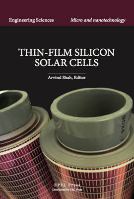
Thin-Film Silicon Solar Cells
Crc Press Inc (Verlag)
978-1-4200-6674-6 (ISBN)
Photovoltaic technology has now developed to the extent that it is close to fulfilling the vision of a "solar-energy world," as devices based on this technology are becoming efficient, low-cost and durable. This book provides a comprehensive treatment of thin-film silicon, a prevalent PV material, in terms of its semiconductor nature, starting out with the physical properties, but concentrating on device applications. A special emphasis is given to amorphous silicon and microcrystalline silicon as photovoltaic materials, along with a model that allows these systems to be physically described in the simplest manner possible, thus allowing the student or scientist/engineer entering the field of thin-film electronics to master a few basic concepts that are distinct from those in the field of conventional semiconductors. The main part of the book deals with solar cells and modules by illustrating the basic functioning of these devices, along with their limitations, design optimization, testing and fabrication methods. Among the manufacturing processes discussed are plasma-assisted and hot-wire deposition, sputtering, and structuring techniques.
Arvind V. Shah studied in Bombay, London and Zürich, receiving his Ph.D. in Applied Physics in 1968 from the Swiss Federal Institute of Technology in Zurich (ETH). He worked at the ETH until founding the Centre for Electronics Design and Technology (CEDT) at the Indian Institute of Science, Bangalore, India, in 1975. In March 1979, he was appointed professor of electronics at the University of Neuchâtel, and in 1988 began a concurrent, part-time appointment at the Swiss Federal Institute of Technology in Lausanne (EPFL). He is founder of Thin-film and Photovoltaics Laboratory at IMT Neuchâtel where he was involved with the invention of VHF plasma deposition and the pioneering work with microcrystalline silicon and “micromorph” tandem solar cells. Since 2000, he has been involved in the successful industrial transfer of technology, negotiating major licensing agreements both to start-up and established companies.
Introduction; Christophe Ballif
Explaining the role of thin-film silicon within PV today and tomorrow
Basic Properties of amorphous silicon (a-Si); Arvind Shah and Wolfhard Beyer
Structure of amorphous silicon
"Free" and "trapped" carriers (electrons and holes), mobility gap
Gap states
Optical absorption; optical gap and sub-bandgap absorption
Transport, conductivity and recombination
Doping of amorphous silicon layers
Hydrogen in amorphous silicon layers; Wolfhard Beyer
Alloys (with Germanium and Carbon); Wolfhard Beyer
Conclusions
Basic properties of hydrogenated µc-Si:H; Friedhelm Finger
History
Structural properties of µc-Si:H
Optical properties
Electrical properties and transport
Metastabilty -- Instabilty
Comparison with amorphous silicon
Alloys (ongoing research work)
Conclusions
Theory of solar cell devices; Arvind Shah, Corinne Droz and Martin Python
Conversion of light into electrical carriers by a semi-conductor diode
The "pn-type" or "classical" diode: Dark characteristics
The "pn-type" or "classical" diode: Properties under illumination
Limits on solar cell efficiency η
The "pin-type" diode
Summary and conclusions of theoretical part
Tandem and multi-junction solar cells; Martin Python and Arvind Shah
Introduction; general concept
Principle of two-terminal tandem cell
Practical problems of two-terminal tandem cells
Typical tandem and multi-junction cells
Spectral response (SR) and External Quantum Efficiency (EQE) measurements
Conclusions
Module Fabrication and Performance; Horst Schade and Jean-Eric Bourée
Plasma-enhanced chemical vapor deposition (PECVD)
Hot Wire chemical vapour deposition (HWCVD)
Doped layers
Transparent conductive oxides (TCO) as contact layers
Laser scribing and series connection of cells
Module performance
Module finishing
Conclusions
Application Examples of Solar Cells; Various contributors, edited by Horst Schade and Arvind Shah
Building-integrated photovoltaics (BIPV) - aspects and examples
Stand-alone and portable applications (Oppizzi)
Indoor applications of a-Si solar cells; J. Randall
Space Applications; N. Wyrsch
Conclusions
Large-area thin-film Electronics; Nicolas Wyrsch
Thin-film transistors (TFTs) and Display Technology
Large-area imagers
Thin-film sensors on C-MOS Chips (Light imagers, Particle sensors, particle imagers)
Conclusions
| Erscheint lt. Verlag | 15.4.2021 |
|---|---|
| Verlagsort | Bosa Roca |
| Sprache | englisch |
| Maße | 156 x 235 mm |
| Gewicht | 1021 g |
| Themenwelt | Naturwissenschaften ► Physik / Astronomie ► Elektrodynamik |
| ISBN-10 | 1-4200-6674-9 / 1420066749 |
| ISBN-13 | 978-1-4200-6674-6 / 9781420066746 |
| Zustand | Neuware |
| Haben Sie eine Frage zum Produkt? |
aus dem Bereich


