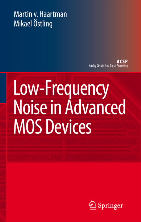
Low-Frequency Noise in Advanced MOS Devices
Springer-Verlag New York Inc.
978-1-4020-5909-4 (ISBN)
The Book will be based on the following work which also is the publication list for Dr Martin von Haartman; Ph. D. Thesis: Low-frequency noise characterization, evaluation and modeling of advanced Si- and SiGe-based CMOS transistors, xx, 124 pages, 9 appended papers, Stockholm, April 2006. http://www.diva-portal.org/kth/theses/abstract.xsql?dbid=3888 Journals: M. von Haartman, D. Wu, B. G. Malm, P.-E. Hellström, S.-L. Zhang and M. Östling, "Low-frequency noise in Si0.7Ge0.3 surface channel pMOSFETs with ALD HfO2/Al2O3 gate dielectrics", Solid-State Electronics, vol. 48, pp. 2271-2275, 2004. D. Wu, M. von Haartman, J. Seger, E. Tois, M. Tuominen, P.-E. Hellström, M. Östling, S.-L. Zhang, "Ni-salicided CMOS with a poly-SiGe/Al2O3/HfO2/Al2O3 gate stack", Microelectron Eng., vol. 77, pp. 36-41, 2005. M. von Haartman, J. Westlinder, D. Wu, B. G. Malm, P.-E. Hellström, J. Olsson, S.-L. Zhang, M. Östling, "Investigation of low-frequency noise and Coulomb scattering in Si0.8Ge0.2 surface channel pMOSFETs with ALD Al2O3 gate dielectrics", Solid-State Electronics, vol. 49, pp. 907-914, 2005. J. Seger, P.-E. Hellström, J. Lu, B. G. Malm, M. von Haartman, M. Östling, and S.-L. Zhang, "Lateral enroachment of Ni-silicide in the source/drain regions on ultra-thin silicon-on-insulator", Appl. Phys. Lett., vol. 86, 253507, 2005. C. Isheden, P.-E. Hellström, M. von Haartman, H. H. Radamson, and M. Östling, "pMOSFETs with recessed and selectively regrown Si1-xGex source/drain junctions", Mat. Sci. Sem. Proc., vol. 8, pp. 359-362, 2005. M. von Haartman, B. G. Malm, and M. Östling, "A comprehensive study on Low-frequency noise and mobility in Si and SiGe pMOSFETs with high-k gate dielectrics and TiN gate", IEEE Trans. Electron Devices, vol. 53, pp. 836-843,April 2006. J. Hållstedt, M. von Haartman, P.-E. Hellström, M. Östling, and H. H. Radamson, "Hole mobility in ultra thin body SOI pMOSFETs with buried SiGe or SiGeC channels", accepted for publication in IEEE Electron Device Letters. International conferences: M. von Haartman, J. Hållstedt, J. Seger, B. G. Malm, H. H. Radamson, P.-E. Hellström, and M. Östling, "Low-frequency noise in SiGe channel pMOSFETs on ultra-thin SOI with Ni-silicided Source/Drain", in Proc. 18th Int. Conf. Noise and Fluctuations (ICNF), 2005, pp. 307-310. M. von Haartman, B. G. Malm, P.-E. Hellström, and M. Östling, "Noise in Si-based MOSFETs with high-k gate dielectrics", in Proc. 18th Int. Conf. Noise and Fluctuations (ICNF), 2005, pp. 225-230. (Invited oral presentation) Dr von Haartman also received the following honours: 2001, Gunnar Wallquist Study Medal given to the best KTH graduate each year. 2001, Best graduate of the year by the School of Electrical Engineering, KTH. 2004, IEEE Electron Devices Society Graduate Student Fellowship CV for Mikael Östling: He has been with the faculty of EE of KTH, Royal Institute of Technology in Stockholm, Sweden since 1984 where he holds a position as professor in solid state electronics. Since 2001 he is head of the department of microelectronics and information technology. In December 2004 he was appointed Dean, School of Information and Communication Technology, KTH. He was a senior visiting Fulbright Scholar 1993-94 with the center for integrated systems at Stanford University, and a visiting professor with the University of Florida, Gainesville. He initiated and was appointed program director by the Swedish Foundation for Strategic Research for a silicon nanoelectronics national program 2000-2007. His research interests are silicon/silicon germanium devices and process technology for very high frequency, as well as devicetechnology for wide bandgap semiconductors with special emphasis on silicon carbide and nitride based structures. He has supervised 20 PhD theses work, and been the author of 8 book chapters and about 300 scientific papers published in international journals and conferences. He is an editor of the IEEE Electron Device Letters and a fellow of the IEEE.
Authors. Preface. Acknowledgments. Chapter 1 Fundamental noise mechanisms. Chapter 2 Noise characterization. Chapter 3 1/f noise in MOSFETs - origins and modelling. Chapter 4 1/f Noise performance of advanced CMOS devices. Chapter 5 Introduction to noise in RF/analog circuits. Appendix I List of Symbols. Appendix II List of Acronyms. Appendix III Solutions to problems. Index.
| Reihe/Serie | Analog Circuits and Signal Processing |
|---|---|
| Zusatzinfo | XVI, 216 p. |
| Verlagsort | New York, NY |
| Sprache | englisch |
| Maße | 155 x 235 mm |
| Themenwelt | Naturwissenschaften ► Physik / Astronomie ► Mechanik |
| Technik ► Elektrotechnik / Energietechnik | |
| ISBN-10 | 1-4020-5909-4 / 1402059094 |
| ISBN-13 | 978-1-4020-5909-4 / 9781402059094 |
| Zustand | Neuware |
| Haben Sie eine Frage zum Produkt? |
aus dem Bereich


