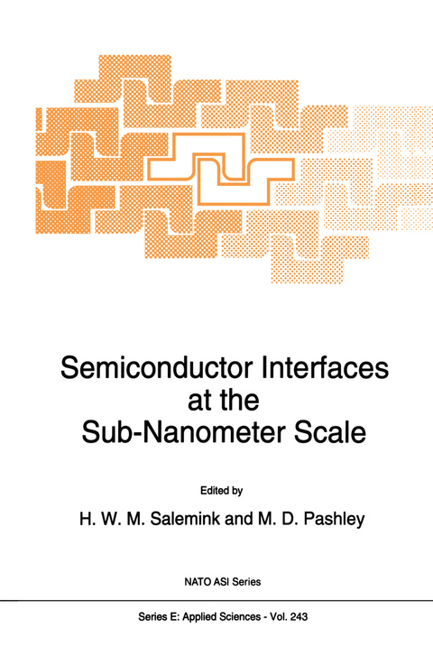
Semiconductor Interfaces at the Sub-Nanometer Scale
Springer (Verlag)
978-0-7923-2397-6 (ISBN)
The Advanced Research Workshop on the Physical Properties of Semiconductor Interfaces at the Sub-Nanometer Scale was held from 31 August to 2 September, 1992, in Riva del Garda. Italy. The aim of the workshop was to bring together experts in different aspects of the study of semiconductor interfaces and in small-scale devices where the interface properties can be very significant It was our aim that this would help focus research of the growth and characterization of semiconductor interfaces at the atomic scale on the issues that will have the greatest impact on devices of the future. Some 30 participants from industrial and academic research institutes and from 11 countries contributed to the workshop with papers on their recent wode. . 'There was ample time for discussion after each talk. as well as a summary discussion at the end of the meeting. The major themes of the meeting are described below. The meeting included several talks relating to the different growth techniques used in heteroepitaxial growth of semiconductors. Horikoshi discussed the atomistic processes involved in MBE, MEE and MOCVD, presenting results of experimental RHEED and photoluminescence measurements; Foxon compared the merits of MBE, MOCVD, and eBE growth; Molder described RHEED studies of Si/Ge growth by GSMBE, and Pashley discussed the role of surface reconstructions in MBE growth as seen from STM studies on GaAs. On the theoretical side, Vvedensky described several different methods to model growth: molecular dynamics, Monte Carlo techniques, and analytic modeling.
I. Epitaxial Growth of Semiconductors.- “Surface Atomic Processes during Epitaxial Growth”.- “Formation Mechanism of CuPt-Type Sublattice Ordering for III-III-V Type Compound Semiconductors”.- “Surface Chemistry in the Si/Ge GSMBE System Studied Using RHEED”.- “Diffusion of Si in ?-Doped GaAs Studied by Magneto Transport”.- “Theory of Atomic-Scale Processes during Epitaxial Growth: Current Status”.- “A Comparison of Growth by Molecular Beam Epitaxy, Metalorganic Chemical Vapour Deposition and Chemical Beam Epitaxy”.- “The Role of Surface Reconstructions in MBE Growth of GaAs”.- “A Lattice Gas Analysis of Binary Alloys on a Tetrahedral Lattice”.- “Resonant Tunnelling via the Bound States of Shallow Donors”.- II. Electronic Properties of Semiconductor Interfaces.- “Engineering of Semiconductor Heterostructures by Ultrathin Control Layers”.- “Interface Chemical Structure, Band Offsets and Optical Properties of Various III-V Compounds Heterostructures”.- “Dipole Layers at GaAs Heterojunctions and Their Investigation”.- “Clustering and Correlations on GaAs-Metal Interface”.- III. Atomic Scale Analysis of Semiconductor Interfaces.- “Cross-Sectional Scanning Tunneling Microscopy of GaAs Doping Superlattices: Pinned vs. Unpinned Surfaces”.- “Semiconductor Interfaces: Structure, Properties and Processing at the Atomic Level”.- “Epitaxial Interfaces of III-V Heterostructures: Atomic Resolution, Composition Fluctuations and Doping”.- IV. Group IV Materials.- “Group IV Strained Layer Systems”.- “MISFIT Accommodation during Heteroepitaxial Growth”.- “Smear-Out of the Ge/Si Interface in Gas Source MBE Monitored by RHEED”.- “Optical Properties of Imperfect Si-Ge Heterostructures”.- “Si1-x-yGexCy Growthand Properties of the Ternary System”.- “Atomic-Scale View of Epitaxial Layers with Cross-Sectional Scanning Tunneling Microscopy”.- V. Nanometer Scale Devices.- “Atomic-Scale Understanding and Controllability of Heterointerfaces in Quantum Microstructures”.- “Do Periodic Interface Corrugations Cause the Unusual Optical Properties of GaAs/AlAs Heterostructures Grown on Non-(100)-Oriented Substrates?”.- “Strained Layer Quantum Well Semiconductor Lasers”.- List of Participants.
| Erscheint lt. Verlag | 31.7.1993 |
|---|---|
| Reihe/Serie | NATO Science Series E ; 243 |
| Zusatzinfo | XI, 256 p. |
| Verlagsort | Dordrecht |
| Sprache | englisch |
| Maße | 155 x 235 mm |
| Themenwelt | Naturwissenschaften ► Chemie ► Analytische Chemie |
| Naturwissenschaften ► Physik / Astronomie ► Elektrodynamik | |
| Naturwissenschaften ► Physik / Astronomie ► Festkörperphysik | |
| Technik ► Maschinenbau | |
| ISBN-10 | 0-7923-2397-1 / 0792323971 |
| ISBN-13 | 978-0-7923-2397-6 / 9780792323976 |
| Zustand | Neuware |
| Informationen gemäß Produktsicherheitsverordnung (GPSR) | |
| Haben Sie eine Frage zum Produkt? |
aus dem Bereich


