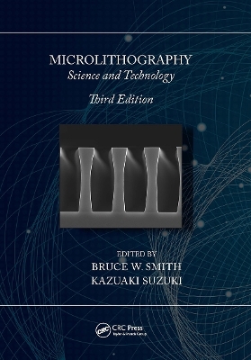
Microlithography
CRC Press (Verlag)
978-1-032-83673-7 (ISBN)
The completely revised Third Edition to the bestselling Microlithography: Science and Technology provides a balanced treatment of theoretical and operational considerations, from fundamental principles to advanced topics of nanoscale lithography. The book is divided into chapters covering all important aspects related to the imaging, materials, and processes that have been necessary to drive semiconductor lithography toward nanometer-scale generations. Renowned experts from the world�€�s leading academic and industrial organizations have provided in-depth coverage of the technologies involved in optical, deep-ultraviolet (DUV), immersion, multiple patterning, extreme ultraviolet (EUV), maskless, nanoimprint, and directed self-assembly lithography, together with comprehensive descriptions of the advanced materials and processes involved.
New in the Third Edition
In addition to the full revision of existing chapters, this new Third Edition features coverage of the technologies that have emerged over the past several years, including multiple patterning lithography, design for manufacturing, design process technology co-optimization, maskless lithography, and directed self-assembly. New advances in lithography modeling are covered as well as fully updated information detailing the new technologies, systems, materials, and processes for optical UV, DUV, immersion, and EUV lithography.
The Third Edition of Microlithography: Science and Technology authoritatively covers the science and engineering involved in the latest generations of microlithography and looks ahead to the future systems and technologies that will bring the next generations to fruition.
Loaded with illustrations, equations, tables, and time-saving references to the most current technology, this book is the most comprehensive and reliable source for anyone, from student to seasoned professional, looking to better understand the complex world of microlithography science and technology.
Bruce W. Smith is a Distinguished Professor of engineering at the Rochester Institute of Technology. He has been involved in teaching and research in microelectronic and microsystems engineering for over 35 years. His areas of research include semiconductor processing, deep ultraviolet (DUV), vacuum ultraviolet (VUV), immersion, and extreme ultraviolet (EUV) lithography, thin films, optics, and microelectronic materials. He has authored over 250 technical publications, given over 100 technical talks, and received over 25 patents, licensing his technology both nationally and internationally. He has worked extensively with individuals and organizations in the semiconductor industry, including industrial partners in the Semiconductor Research Corporation, SEMATECH, and the IMEC. He is the recipient of numerous teaching and research awards, including the Institute of Electrical and Electronics Engineers (IEEE) Technical Excellence Award, the American Vacuum Society (AVS) Excellence in Leadership Award, the Society for Photo-optical Instrumentation Engineers (SPIE) Research Mentoring Award, and the Rochester Institute of Technology Trustees Scholarship Award. He has also been inducted into the Rochester Institute of Technology Innovator Hall of Fame. Professor Smith is a Fellow of the Institute of Electrical and Electronics Engineers, the Optical Society of America, and the Society for Photo-optical Instrumentation Engineers. Kazuaki Suzuki majored in plasma physics and X-ray astronomy in the University of Tokyo, Japan. He has been a project manager for developing new concept exposure tools at Nikon Corporation, such as the early-generation KrF excimer laser stepper, the first-generation KrF excimer laser scanner, the electron beam projection exposure system, and the full-field extreme ultraviolet scanner. He received his Ph. D. in Precision Engineering from the University of Tokyo about the system design of exposure tools for microlithography. He has authored and coauthored many papers in the field of exposure tool and related technologies, including advanced equipment control by using metrology data. He also holds numerous patents in the same field. In the first decade of this century, he was a member of the program committee of the Society for Photo-optical Instrumentation Engineers (SPIE) Microlithography and other international conferences such as Micro & Nano Engineering in Europe and the International Microprocesses and Nanotechnology Conference in Japan. He was one of the associate editors of Journal of Micro/Nanolithography, MEMS, and MOEMS (JM3) from 2002 to 2009. He moved to Tokyo Tech Academy for Convergence of Materials and Informatics at Tokyo Institute of Technology (Tokyo Tech) in March 2019.
Chapter 1 Lithography, Etch, and Silicon Process Technology Chapter 2 Optical Nanolithography Chapter 3 Multiple Patterning Lithography Chapter 4 EUV Lithography Chapter 5 Alignment and Overlay Chapter 6 Design for Manufacturing and Design Process Technology Co-Optimization Chapter 7 Chemistry of Photoresist Materials Chapter 8 Photoresist and Materials Processing Chapter 9 Optical Lithography Modeling Chapter 10 Maskless Lithography Chapter 11 Imprint Lithography Chapter 12 Metrology for Nanolithography Chapter 13 Directed Self-Assembly of Block Copolymers
| Erscheinungsdatum | 23.08.2024 |
|---|---|
| Zusatzinfo | 570 Illustrations, black and white |
| Verlagsort | London |
| Sprache | englisch |
| Maße | 178 x 254 mm |
| Gewicht | 1660 g |
| Themenwelt | Naturwissenschaften ► Physik / Astronomie ► Optik |
| Technik ► Elektrotechnik / Energietechnik | |
| ISBN-10 | 1-032-83673-3 / 1032836733 |
| ISBN-13 | 978-1-032-83673-7 / 9781032836737 |
| Zustand | Neuware |
| Informationen gemäß Produktsicherheitsverordnung (GPSR) | |
| Haben Sie eine Frage zum Produkt? |
aus dem Bereich


